
Analog systems and applications, lecture — X.
This article belongs to a series of lectures on analog electronics, the paper goes by the name “Analog Systems and Applications” for the physics honors degree class. All lectures of this series will be found here. This comprises of the 10th lecture of the series. The lecture was delivered on 8th February 2018.
Full wave rectifier — Center tapped type.
In our last two lecture we discussed in all detail the half wave rectifier which is constructed from an ideal diode and studied its various parameters such as its rectifier efficiency and transformer utilization factor. Please have a look at these lectures as the same will have an indubitable bearing on what we will discuss today. Today we will discuss the case of a full wave rectifier. But there are two ways such a rectifier can be constructed and we will focus for today the logical choice of center tapped full wave rectifier before we delve into the next choice of Bridge type full wave rectifier.
The diagram for a center tapped full wave rectifier is shown below.
The center tapped full wave rectifier.
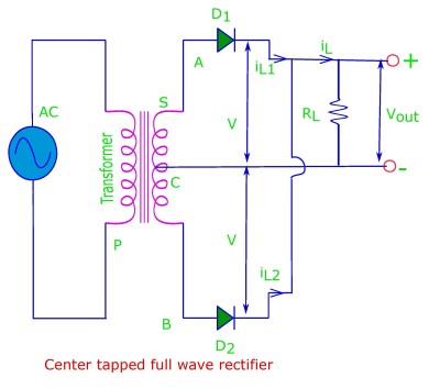
(i) Two diodes are used instead of one in case of half-wave rectifier. Lets call’em D1 and D2.
(ii) Power transformer is centrally tapped, at C, at secondary.
(iii) Diodes are connected together and in common to one end of the load RL. Other end of the load RL is connected to central tapping from C.
(iv) Half of potential (voltage) of secondary coils of transformer appears across each diode. C is the reference of zero level of voltage from the AC voltage signal of the secondary coils.
(v) In the first half cycle if A is at positive potential, D1 is forward and D2 is reverse biased. The opposite is true for second half cycle, here D1 is reverse and D2 is forward biased.
The output across load produces a full wave. In each half cycle direction of current across RL is same.
Let V = V0 sin ω t be applied alternating potential at each diode and Rf be the dynamic resistance in forward bias as in the case of half wave rectifier. Similarly let Rs be the resistance of the secondary coils. Then current iL across RL is sum of currents iL1 and iL2 emanating from D1 and D2.


Also: 
Average or DC value of I and V.
![I_{dc}=\frac{1}{T} \int_0^{T/2}i_{L_{1}} dt + \frac{1}{T} \int_{T/2}^{T}i_{L_{2}} dt =\frac{1}{T} \Big[ \int_0^{T/2}I_0 \sin \omega t dt + \int_{T/2}^{T}(-I_0 \sin \omega t dt) \Big ]](https://s0.wp.com/latex.php?latex=I_%7Bdc%7D%3D%5Cfrac%7B1%7D%7BT%7D+%5Cint_0%5E%7BT%2F2%7Di_%7BL_%7B1%7D%7D+dt+%2B+%5Cfrac%7B1%7D%7BT%7D+%5Cint_%7BT%2F2%7D%5E%7BT%7Di_%7BL_%7B2%7D%7D+dt+%3D%5Cfrac%7B1%7D%7BT%7D+%5CBig%5B+%5Cint_0%5E%7BT%2F2%7DI_0+%5Csin+%5Comega+t+dt+%2B+%5Cint_%7BT%2F2%7D%5E%7BT%7D%28-I_0+%5Csin+%5Comega+t+dt%29+%5CBig+%5D&bg=ffffff&fg=cd5c5c&s=1&c=20201002)

So, ![\boxed{V_{dc}=I_{dc}R_L=\frac{2I_0 R_L}{\pi}=\frac{2V_0 R_L}{\pi(R_f+R_s+R_L)}=\frac{2V_0}{\pi \big[1+\frac{R_f+R_s}{R_L} \big]}}](https://s0.wp.com/latex.php?latex=%5Cboxed%7BV_%7Bdc%7D%3DI_%7Bdc%7DR_L%3D%5Cfrac%7B2I_0+R_L%7D%7B%5Cpi%7D%3D%5Cfrac%7B2V_0+R_L%7D%7B%5Cpi%28R_f%2BR_s%2BR_L%29%7D%3D%5Cfrac%7B2V_0%7D%7B%5Cpi+%5Cbig%5B1%2B%5Cfrac%7BR_f%2BR_s%7D%7BR_L%7D+%5Cbig%5D%7D%7D+&bg=ffffff&fg=cd5c5c&s=0&c=20201002)
Power is given by: 
RMS value of current.

So, 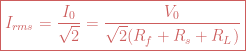
Fourier analysis of output frequencies.
![i_{L_{1}} = I_0 \Big[ \frac{1}{\pi} + \frac{1}{2} \sin \omega t -\frac{2}{3\pi}\cos 2 \omega t - \frac{2}{15 \pi}\cos 4 \omega t + ...\Big]](https://s0.wp.com/latex.php?latex=i_%7BL_%7B1%7D%7D+%3D+I_0+%5CBig%5B+%5Cfrac%7B1%7D%7B%5Cpi%7D+%2B+%5Cfrac%7B1%7D%7B2%7D+%5Csin+%5Comega+t+-%5Cfrac%7B2%7D%7B3%5Cpi%7D%5Ccos+2+%5Comega+t+-+%5Cfrac%7B2%7D%7B15+%5Cpi%7D%5Ccos+4+%5Comega+t+%2B+...%5CBig%5D&bg=ffffff&fg=cd5c5c&s=0&c=20201002)
![i_{L_{2}} = I_0 \Big[ \frac{1}{\pi} - \frac{1}{2} \sin \omega t -\frac{2}{3\pi}\cos 2 \omega t - \frac{2}{15 \pi}\cos 4 \omega t + ...\Big]](https://s0.wp.com/latex.php?latex=i_%7BL_%7B2%7D%7D+%3D+I_0+%5CBig%5B+%5Cfrac%7B1%7D%7B%5Cpi%7D+-+%5Cfrac%7B1%7D%7B2%7D+%5Csin+%5Comega+t+-%5Cfrac%7B2%7D%7B3%5Cpi%7D%5Ccos+2+%5Comega+t+-+%5Cfrac%7B2%7D%7B15+%5Cpi%7D%5Ccos+4+%5Comega+t+%2B+...%5CBig%5D&bg=ffffff&fg=cd5c5c&s=0&c=20201002)
So, ![\boxed{ i_L = I_0 \Big[ \frac{2}{\pi} -\frac{4}{3\pi}\cos 2 \omega t - \frac{4}{15 \pi}\cos 4 \omega t + ...\Big]}](https://s0.wp.com/latex.php?latex=%5Cboxed%7B+i_L+%3D+I_0+%5CBig%5B+%5Cfrac%7B2%7D%7B%5Cpi%7D+-%5Cfrac%7B4%7D%7B3%5Cpi%7D%5Ccos+2+%5Comega+t+-+%5Cfrac%7B4%7D%7B15+%5Cpi%7D%5Ccos+4+%5Comega+t+%2B+...%5CBig%5D%7D&bg=ffffff&fg=cd5c5c&s=0&c=20201002)
Odd harmonics (and fundamental frequency therefore) are removed. Lowest frequency is twice that of input.
Rectifier efficiency.

Therefore the theoretical maximum efficiency is 81.06 % but the maximum efficiency at maximum output power is 40.53 %. (see lecture IX to read the explanation of this conclusion).
Transformer utilization factor.
Pac (rated) = {Pac (rated)}1st half + Pac (rated) = {Pac (rated)}2nd half .

V0 = I0 (Rf +Rs +RL).
![TUF_{secondary}=\frac{P_{dc}}{P_{ac}(rated)}=\frac{I_{dc}^2R_L}{\frac{V_0I_0}{\sqrt 2}}\\ \\=\frac{(2I_0 / \pi)^2R_L}{I_0^2 (R_f+R_s+R_L)/\sqrt 2} =\frac{4\sqrt 2}{\pi^2}\frac{R_L}{R_f+R_s+R_L}\\ \\ =0.573\big[1+\frac{R_f+R_s}{R_L}\big]^{-1}\approx 0.573\big[1-\frac{R_f+R_s}{R_L}\big]\approx 0.573](https://s0.wp.com/latex.php?latex=TUF_%7Bsecondary%7D%3D%5Cfrac%7BP_%7Bdc%7D%7D%7BP_%7Bac%7D%28rated%29%7D%3D%5Cfrac%7BI_%7Bdc%7D%5E2R_L%7D%7B%5Cfrac%7BV_0I_0%7D%7B%5Csqrt+2%7D%7D%5C%5C+%5C%5C%3D%5Cfrac%7B%282I_0+%2F+%5Cpi%29%5E2R_L%7D%7BI_0%5E2+%28R_f%2BR_s%2BR_L%29%2F%5Csqrt+2%7D+%3D%5Cfrac%7B4%5Csqrt+2%7D%7B%5Cpi%5E2%7D%5Cfrac%7BR_L%7D%7BR_f%2BR_s%2BR_L%7D%5C%5C+%5C%5C+%3D0.573%5Cbig%5B1%2B%5Cfrac%7BR_f%2BR_s%7D%7BR_L%7D%5Cbig%5D%5E%7B-1%7D%5Capprox+0.573%5Cbig%5B1-%5Cfrac%7BR_f%2BR_s%7D%7BR_L%7D%5Cbig%5D%5Capprox+0.573&bg=ffffff&fg=cd5c5c&s=1&c=20201002)
TUFprimary = rectification efficiency.
So TUFprimary = 0.811, TUFaverage= 1/2 [TUFprimary + TUFsecondary] = 1/2(0.573+0.811) = 0.692.
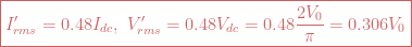
Ripple factor.
Then ripple factor is given by: ![r = \frac{I_{rms}'}{I_{dc}} = \big(\frac{I_{rms}^2}{I_{dc}^2}-1\big)^{\frac{1}{2}}=\bigg[\frac{(I_0 /\sqrt 2)^2}{(2 I_0/\pi)^2}-1\bigg]^{\frac{1}{2}}=(1.1107^2-1)^{\frac{1}{2}}=0.48](https://s0.wp.com/latex.php?latex=r+%3D+%5Cfrac%7BI_%7Brms%7D%27%7D%7BI_%7Bdc%7D%7D+%3D+%5Cbig%28%5Cfrac%7BI_%7Brms%7D%5E2%7D%7BI_%7Bdc%7D%5E2%7D-1%5Cbig%29%5E%7B%5Cfrac%7B1%7D%7B2%7D%7D%3D%5Cbigg%5B%5Cfrac%7B%28I_0+%2F%5Csqrt+2%29%5E2%7D%7B%282+I_0%2F%5Cpi%29%5E2%7D-1%5Cbigg%5D%5E%7B%5Cfrac%7B1%7D%7B2%7D%7D%3D%281.1107%5E2-1%29%5E%7B%5Cfrac%7B1%7D%7B2%7D%7D%3D0.48&bg=ffffff&fg=cd5c5c&s=1&c=20201002)
Peak Inverse Voltage.
According to Kirchhoff’s law: VD1 – VD2 + 2 V0 sin ωt = 0. When is D1 is conducting, VD1 = 0, this implies VD2 = 2 V0 sin ωt. So (VD2)max = 2 V0. Similarly when D2 is conducting, VD2 = 0, (VD1)max = 2 V0.
Voltage Regulation.
V.R. = {(Vdc)NL – (Vdc)FL}/(Vdc)FL.

So, 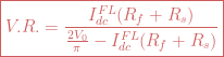
Home work.
Compare a full wave and a half wave rectifier on the basis of their average (dc), rms frequency terms, efficiency, ripple factor, PIV and VR. Make a table such as the following.
| half wave | CT full wave | remarks | |
| Quantity |

Leave a comment