Analog systems and applications — lecture-XIV.
Photo-diodes, lecture-XIV.
This article belongs to a series of lectures on analog electronics, the paper goes by the name “Analog Systems and Applications” for the physics honors degree class. All lectures of this series will be found here. This is the 14th lecture of the series. The lecture was delivered on 8th March 2018.
Photodiodes.
In our last lecture we discussed the concept and working of a particular type of diode which gets an immense application in solid state lighting technology in today’s world: the light emitting diode or the LED in short. There we saw how its capable of converting the electrical energy into optical energy. There is yet another type of diode which is the exact opposite in terms of this mechanism, it converts optical energy into electrical energy.
Together these two types of devices are known as optoelectronics devices, as either way optical and electrical energy are its input or output. Another type of diode that falls into the former category same as that of LED is LASER diode. In the opposite kind there are two examples we can cite: the photo-diode and the solar cell. They both take in light as an input of energy and convert that into electrical energy.
Today we will focus on the photodiodes.
A photodiode is a semiconductor device which generates electric energy by consuming light energy. It is also known as a photo-detector, a photo-sensor or a light-detector.
(i) Photodiodes operate under reverse bias condition. Remember the LED operate under forward bias.
(ii) Photodiodes are highly sensitive to light. When photons fall on photodiodes they are easily converted into electric energy. Solar cells are based on this principle of photodiode. But solar cells operate only at bright light. Therefore they are known as “large area photodiode”.
(iii) Construction and workings of photodiodes are very similar to that of pn junction diode. In pn junction diodes only voltage is used as energy source. But in a photodiode both voltage and light can be used as energy source.
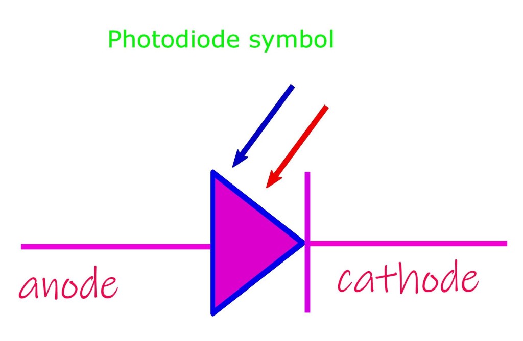
Symbol.
Here is the representative symbol of a photodiode as its used in electric/electronics circuits. The arrows here are reversed wrt how they are shown in the symbol for light emitting diode. The arrows here represent the fact that light or photon is being incident on the diode.
The representative symbol for a photodiode in any electronic or electrical circuit is same as that for a light emitting diode except the arrows point towards the diode rather than away from it.

Photodiode characteristics and conditions.
(i) Always operated in reverse bias.
(ii) Applied reverse bias voltage should be low.
(iii) It should generate low noise.
(iv) It should have high gain.
(v) It should have high response speed.
(vi) It should be highly sensitive to light.
(vii) It should be less sensitive to temperature.
(viii) It should be inexpensive, small in size, and be highly durable.
Working of photodiodes.
Normal pn junction diodes (read about them here and here) allow a small amount of electric current, under reverse bias (which is known as reverse saturation current). In order to have a higher value of current, under reverse bias, we need to generate more number of minority carriers. External reverse voltage imparts energy to minority carriers but it does not enhance their population.
A small number of minority carriers are produced due to external reverse voltage. But these carriers recombine with the opposite carriers before crossing the pn junction, i.e. in their respective region, (Holes in N-region, where they are in minority and free electrons in P-region where they are in minority, recombine there). Thus no electric current flows due to these charge carriers.
By applying external energy directly to the depletion region, more number of charge carriers can be generated. In photodiodes, light energy is used as an external energy source to generate electron-hole-pairs (EHP) in the depletion layer.
Types of photodiodes.
There are 3 types of photodiodes.
(i) PN junction photodiodes: A P and a N type layer is used for such photodiodes.
(ii) PIN photodiodes: Here a P-layer and a N-layer accommodate an intrinsic (i.e. undoped) layer in-between. This increases the response speed of the diode and the application device where such a photodiode is used.
(iii) Avalanche photodiodes: High reverse voltage is applied to achieve avalanche multiplication in such photodiodes.
PN junction photodiodes.
(i) When light falls on this type of photodiodes, valence electrons in the depletion region gain energy.
(ii) If incident photon energy is > band-gap of semiconductor material used (hν > Eg), valence electrons gain enough energy., break the covalent bonding with parent atoms and become free electrons. Thus EHP are created. This process is known as “inner photoelectric effect” (the generation of EHP by the application of light energy).
(iii) The strong depletion region electric field and external electric field increase the drift velocity of the electrons and holes and they can easily cross the pn junction before recombination can take place. This increases minority carrier current.
(iv) When no light is applied to the reverse biased photodiode, it carries a small reverse current due to external voltage. This current is known as “dark current” and its denoted as: Iλ.
(v) Reverse current is independent of applied reverse bias voltage but depends upon light intensity.
(vi) The total current in the photodiode is thus the sum of dark-current and photo-current (current due to application of light).
PIN photodiode.
(i) It is similar to PN junction photodiode but the PIN photodiodes improve the photodiode performance.
(ii) PIN photodiodes increase minority current thereby response speed (for the same amount of light energy consumed by a pn photodiode).
(iii) In PIN photodiodes there is an extra layer sandwiched between the p and the n layers. The extra layer is made up of intrinsic type material so there are no (free) electric charge carriers to carry current.
(iv) Under reverse bias majority carriers (i.e. holes in p-layer and electrons in n-layer) would not carry any current. But the reverse bias increases the depletion layer width.
(v) The small number of minority carriers (eg produced due to thermal excitation) carry the current under reverse bias.
(vi) When PIN type photodiodes are irradiated with light, a large number of minority carriers are created in the depletion layer.
(vii) PIN photodiode carry large minority carrier current than PN photodiode.
(viii) Under forward bias PIN photodiode behaves like a resistor.
HW: Find out why PIN photodiodes have lesser capacitance compared to PN photodiodes.

Leave a comment