Analog systems and applications, lecture — VII.
Current and resistance in pn junction diodes, Lecture-VII.
This article belongs to a series of lectures on analog electronics, the paper goes by the name “Analog Systems and Applications” for the physics honors degree class. All lectures of this series will be found here. This is the seventh lecture of this series. This particular lecture was delivered on 30th January 2018.
Current flows in a pn junction diode under the application of external potential. The application of such a potential is known as “biasing“. The resulting Poisson’s equation becomes a nonlinear differential equation, i.e. charge concentrations now depend upon the potential. But the potential V (or Φ) now is a function of ‘x‘ (location). Thus the charge concentrations are now different in different regions.
Know more about Poisson’s equation in pn junction context here.
Biasing is of two types. i. Forward bias and ii. Reverse bias.
Forward bias.
When positive terminal of the battery is connected to the p-side of the diode and negative terminal of the battery is connected to the n-side of the diode such a biasing is known as “Forward bias“.
Under forward bias
i. Majority carriers are repelled towards the junction simultaneously. Holes are pushed away by the +ve terminal towards the junction. Similarly electrons are pushed away by the -ve terminal (of battery) towards the junction.
ii. There is resistance offered to this flow by the builtin or contact potential (also known as junction potential barrier) denoted by VB. The applied potential in a forward bias helps the majority carriers overcome this barrier.
iii. In the depletion region recombination of electrons and holes takes place. At the same time holes and electrons could be created in large numbers (due to thermal agitation). This latter is known as regeneration.
iv. There is a “large forward current” (from p-side to n-side in terms of conventional i.e. positive current) during forward bias.
v. Regenerated holes and electrons could enter the depletion region. This reduces the barrier width (x0) as well as effectively the barrier height (energy hill). So V = VB – Vapplied.
Reverse bias.
When negative terminal of the battery is connected to the p-side of the diode and positive terminal of the battery is connected to the n-side of the diode such a biasing is known as “Reverse bias“.
Under reverse bias
i. Majority carrier in p-side (holes) are attracted towards the negative terminal of battery. Similarly majority carriers in n-side (electrons) are attracted by the positive terminal of the battery.
ii. The barrier height and width increases as the free carriers are pushed away from depletion region. There is high resistance and flow of current is almost stopped.
iii. There are a small number of regenerated electrons and holes due to thermal energy. This produces a feeble current known as reverse saturation current. This current is called saturation current as it does not depend upon the value of applied potential (i.e. bias). There is also a current known as surface leakage current (which is produced due to excessive holes present at the surface of the crystal).
iv. Both these current amount to only 10-7 to 10-4 of the forward bias current.
Thus due to biasing the diode essentially allows current only in the forward direction. Due to avalanche effect (which we have discussed earlier, here (last 2 paragraphs on breakdown in reverse bias), the resistance offered in the reverse region becomes very low when applied reverse voltage is very high. So in general in forward and reverse currents, resistance is low in high current regions and high in low current regions.
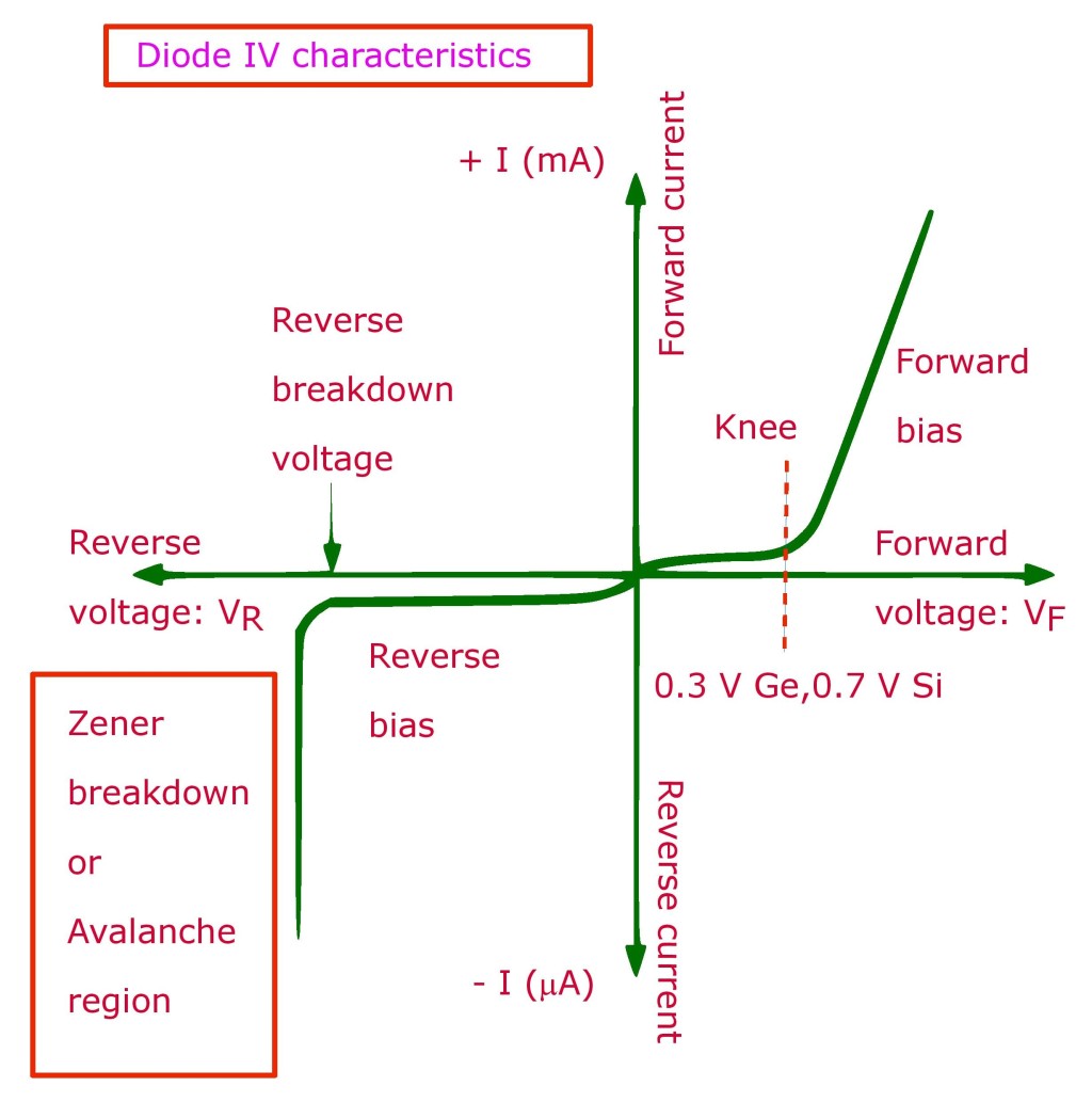
IV characteristics of a pn junction diode in forward and reverse bias conditions.

Diode resistance.
Forward resistance is of two types depending upon the type of applied potential in biasing. If DC source is used for biasing such a resistance is known as static or DC resistance. Similarly if AC source is used for biasing then the resulting resistance is known as dynamic or AC resistance. Lets discuss them in a little more detail.
DC/static resistance
The resistance of the diode is non-linear. i.e. it depends on the point of operation. Its given by: RDC = VDC / IDC.
For forward biasing the DC resistance is denoted as RF and for reverse bias it is denoted as RR. RF is very high at the “knee” and below. When current increases with voltage RF is lowered. RR is quite high (mega ohms order) and decreases when we approach breakdown voltage.
AC/dynamic resistance
Here a constant voltage source is modulated by an ac signal. If Q is the operating point, then instantaneous operating point moves up and down Q. The slope at Q gives the AC resistance and its given by: rd = ΔVd / ΔId. Average AC resistance is defined between two points by drawing a straight-line between them.

The forward dynamic resistance depends on an operational point and the instantaneous value of the ratio of voltage to current. For an average value any two points can be chosen and a straight line can be drawn between the two giving the slope of the line is equivalent to inverse of the dynamic resistance in this given diagram.
PN diode equation (or Shockley’s equation or ideal diode equation)
Its derivation is quite involved and we will just discuss its properties. Its given by the expression: 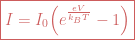
Here V is the barrier potential that we earlier denoted by VB. kB is the Boltzmann constant and T is the absolute temperature, i.e. the temperature expressed in Kelvin. VT = kBT/e corresponds to the mean thermal energy of the particles and called “voltage equivalent of temperature“. At room temperature (i.e. 300 kelvin) VT = 25.88 mV. In this equation. as we will see below, a constant η can also be used: η=1 for Ge and Si, for higher levels of diode current and η=2 for Si and η=1 for Ge for lower levels of diode current.
Forward bias in diode equation
When V > 0, 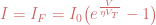
For V >> VT, 

For V = Vth = (forward threshold voltage) = VB, IF ≈ 0. i.e. forward current IF is zero for certain threshold potential (Vth) equal to the barrier potential (VB) and this threshold potential for Ge is 0.3 V and for Si is 0.7 V.
The dynamic forward resistance rF = ΔVF / ΔIF is very small (in the order of ohms). Taking derivative of 

Reverse bias in diode equation
When V < 0, the current is known as “reverse current” 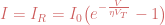
The dynamic reverse resistance (or reverse AC resistance) is given by: rR = ΔVR / ΔIR and → ∞ (in the order of mega-ohms). Thus the pn junction works like a switch (i.e. its an unidirectional device).
Ratio of forward to reverse current at a given applied voltage is known as “rectification ratio“.

Leave a comment