
Analog systems and applications — lecture-XIII.
The Light Emitting Diodes, Lecture-XIII.
This article belongs to a series of lectures on analog electronics, the paper goes by the name “Analog Systems and Applications” for the physics honors degree class. All lectures of this series will be found here. This is the 13th lecture of the series. The lecture was delivered on 27th February 2018.
We have been discussing a lot about what are diodes, their characteristics and their application in the electrical and electronics industry. You must have heard about the durable and power efficient LED bulbs. Do you know they are made from diodes? YES. Semiconductors: they are ubiquitous. Today we will discuss about the light emitting diodes. In short they are called LED. We have grown up seeing them everywhere. Haven’t we? Lighting in marriage parties, TV and mobile handsets to hotel and restaurant decorations.
What is light emitting diode?
Light emitting diodes are diodes which emit either “visible light” or “infrared light” when forward biased. LEDs convert electrical energy input into light energy. Read more about forward bias here.
When LEDs are forward biased, the free electrons in the conduction band, recombine with the holes in the valence band. As a result light of energy equal to the band gap or energy gap of the material used in the diode is released. Materials are so chosen for LEDs that the frequency of light correspond to the frequency of either visible light or infrared light, in the electromagnetic spectrum. You can read more about energy gaps and bands here and here.
The energy corresponding to the band-gap of the material in the medium is given by Eg = hν, where ν is the frequency of the emitted radiation. But frequency and wavelength of any wave are related by the Newton’s velocity of wave formula: ν = c/λ. So wavelength of the emitted radiation is given by: λ = hc/Eg and when expressed in micrometer it has an easy expression to remember which is quite useful: λ (µm)= 1.24/Eg (eV). Just don’t forget to express energy in electron volts.
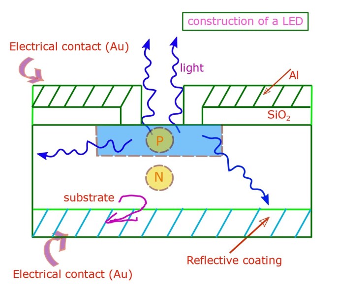
Construction
(i) The N-type layer is grown on a substrate. The P-type layer is deposited on it by the process of diffusion.
(ii) The carrier recombination takes place in the P-layer. Thus the deposition of P-layer is done at the uppermost layer.
(iii) A metal film anode is deposited at the outer edge of the P-layer. This ensures maximum light emission.
(iv) The bottom of the substrate is coated with metal (eg Gold = Au) film. This ensures most of the light is reflected from the surface. This also provides connection to the N-type layer.
Here is a diagram that schematically represents the construction of a light emitting diode.
Schematic representation of the construction of a light emitting diode.
Working
(i) When pn junction is forward biased, barrier width is reduced. It raises the potential energy on the N-side and reduces the same on the P-side.
(ii) Now free electrons and holes (the free charge carriers) have sufficient energy to move to the junction region (space charge layer or depletion layer). The depletion layer is known as active region in case of LED diodes. Its here that recombination of the electrons and holes takes place: producing light of suitable wavelength.
Special nature of LED type diodes.
The LEDs are different from ordinary pn diodes in many respects.
(i) Instead of Si or Ge, they are made from Ga, P and As materials. Si and Ge diodes would release light in the form of heat due to recombination of carriers. This is due to the energy gap of the Si and Ge. Remember the basic formula we mentioned above. λ (µm)= 1.24/Eg (eV). LEDs on the other hand are capable of producing intense visible light.
(ii) In normal silicon diodes energy gap (Eg) between conduction band and valence band edge is small. Only low energy photons are produced. The opposite happens in LED, due to large energy gap between the bands.
(iii) Safe forward voltage ratings of most LED is from 1 V to 3 V and safe current rating is from 100 mA to 200 mA. For normal pn diodes 0.3 V to 0.7 V forward voltages are enough to counteract the potential barriers.
(iv) LED can give off light in various colors. This is not possible with normal pn diodes.
(v) LEDs can be switched off and on really fast (in ‘ns‘ order of time).
Energy band diagram of a light emitting diode.

The following diagram shows how light emitting diodes are represented in symbol in electronics/electrical circuits.
The symbol for a light emitting diode.

Biasing
Large forward or reverse bias voltage can destroy the LED. Thus we need to use current limiting resistor RS to prevent this from happening. (We discussed how this helps in case of Zener diode voltage regulators from exceeding power rating of the diode thereby causing enough concern for its safety in our last lecture.)
The following diagram shows the situation when the diode (LED) is under forward bias (which it must be set to, to produce light). Forward current in LED is IF; IF = (VS–VD)/RS, where VD is the voltage drop across the LED and VS is the source voltage applied.
As VD ~ 2 – 3 volt, energy consumption in LED diodes is higher compared to that in Si or Ge based pn diodes.
Current flowing in a LED due to biasing.

Output characteristics
Amount of light output given out by LED is directly proportional to the amount of forward current passing through the diode. This is shown in the following diagram.
Amount of light output by LED is proportional to current through diode.

Color of light in LED
GaAs (Gallium Arsenide, Red, IR)
Gallium nitride (bright Blue)
Yttrium Aluminum Garnet (White)
Gallium Phosphide (Red, Yellow, Green)
Aluminium Gallium Nitride (UV)
Aluminium Gallium Phosphide (Green)
Advantages
(i) Brightness can be controlled by current. LED can operate at different ambiance of light.
(ii) Consume low energy, inexpensive and easily available, light weight, small and durable.
(iii) Operate very fast.
(iv) No toxic material (no mercury like materials found like in fluorescent lamps).
(v) Emit different colors of light.
Disadvantages
(i) More power consumption than normal pn diodes.
(ii) Luminous efficiency is low for LEDs.
Applications
Burglar alarm system, calculator, traffic signal, digital computers, aviation lighting, digital watch etc.

Leave a comment