Analog systems and applications, lecture — II
“Conductors, semiconductors and holes as charge carriers”
This article belongs to a series of lectures on analog electronics, the paper goes by the name “Analog Systems and Applications” for the physics honors degree class. All lectures of this series will be found here. This is the second lecture of this series. This particular lecture was delivered on 2nd January 2018.
In our last lecture (L-I: lecture-I) we discussed how there are two types of charge carriers in a semiconductor; the electrons and the holes. We also discussed what are intrinsic semiconductors.
i. An intrinsic semiconductor has an equal number of electrons and holes. These are produced due to thermal excitation when an electron is dislodged from the outermost or valence orbit. This is possible as in semiconductors the difference between valence energy level and next higher energy level known as conduction energy level, is small. This difference between valence level and conduction level in energy is known as “energy gap” and its denoted by Eg. Eg for silicon (Si) is nearly 1 eV and for germanium (Ge) is 0.7 eV.
ii. Under the influence of an applied potential difference the electrons move along the direction of positive voltage and the holes move opposite to the applied voltage. The electrons can come out of the crystal and move in the external circuit towards the positive potential. The holes can’t exceed the crystal and as a result can’t come out of the crystal. Any electrons coming from the external circuit can enter the crystal and recombine with a hole.
iii. This maintains a steady flow of electron and hole current. Conductivity of the semiconductor depends on the electrons as well as holes.
Thus the conductivity of the semiconductor can be increased by increasing the concentration of carriers (electrons and holes). This is achieved by DOPING. Doping is the addition of specific impurities to an intrinsic semiconductor. Doped semiconductors are known as “extrinsic semiconductor“.
There are two ways of achieving Doping, ie. increasing carrier concentration by adding suitable impurities.
Increasing concentration of free electrons.
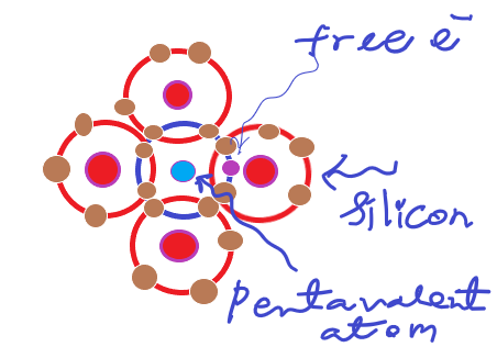
i. A pure silicon crystal is allowed to melt.
ii. The covalent bonds in silicon are broken and silicon transforms from solid to liquid.
iii. Pentavalent atoms such as Antimony (Sb) , Arsenic (As) or Phosphorous (P) are added to molten silicon. These impurities have 5 valence electrons and can add an extra electron to the silicon crystal. Thats why such impurities are known as “Donor atoms/impurities“. The extra electron remains in a higher energy level as 8 electrons already fill the valence shell. Thus its a free electron.
Increasing concentration of holes.
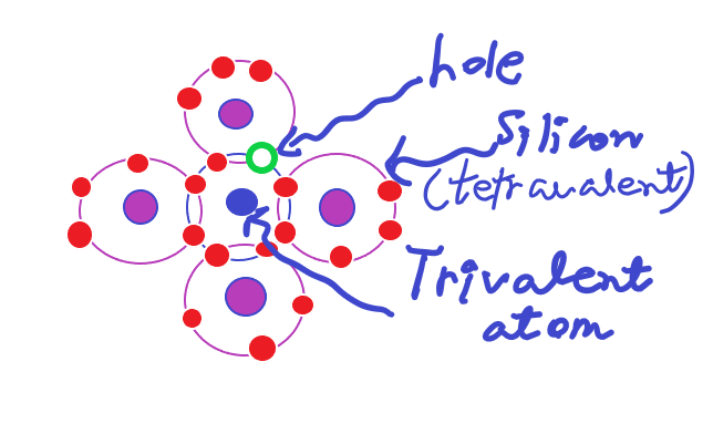
i. We add trivalent impurities such as aluminium (Al), boron (B) or gallium (Ga)to the silicon in its molten state.
ii. Now there are 7 electrons in the valence shell and therefore a “hole” in satisfying the “valence saturation principle“. The holes always remain in the valence energy levels. Trivalent impurities are known as “acceptor atoms/impurities” (they are ready to receive free electrons to satisfy the octet rule of valence saturation).
iii. Addition of trivalent atoms increases the concentration of holes. 
Thus there are two types of extrinsic semiconductors
i. n-type semiconductor: A semiconductor such as silicon which is doped with a pentavalent or donor impurity is known as a n-type semiconductor. n stands for negative. It has an excess of free electronic charge carriers. The free electrons outnumber the holes. Thus electrons in a n-type semiconductor are known as majority carriers and the holes in a n-type semiconductor are known as minority carriers.
ii. p-type semiconductor: A semiconductor such as silicon which is doped with a trivalent or acceptor impurity is known as a p-type semiconductor. p stands for positive. Holes in a p-type semiconductor are much larger in number than free electrons. Thus for a p-type semiconductor holes are known as “majority carriers” and (free) electrons are known as “minority carriers”.
A semiconductor has two bands of energy, the highest occupied energy level is known as valence band. The next higher energy level is known as conduction band.
The energy difference between valence band and conduction band is known as “band gap” or “energy gap” Eg. At T = 0 K valence band of semiconductors is completely filled. Since Eg is small enough, at room temperature (T = 300 K) significant number of electrons can move from the valence band into the conduction band due to thermal excitation. Thus these electrons are free and a hole is created for each electron that moves to the conduction band.
The hole remains in the valence band. The electron moves across the crystal in the conduction band. When an electron falls into a hole, it returns to the valence band by emitting energy as heat, light or radiation. This is the reason LED (light emitting diode) emits light of various colors.
Semiconductors are often categorized on the following basis.
i. Group IV semiconductors. C, Si, Ge and α-Sn found in 4th column of the periodic table with valence electronic configuration: ns2np2.
i. Group III-V semiconductors. 1 element from 3rd column (III) and 1 element from 5th (V). eg GaAs, InSb, GaP, InAs, GaSb. Valence electronic configuration: III; ns2np1. and V; ns2np3.
i. Group II-VI semiconductors. CdS, ZnS.

Leave a comment