Analog systems and applications — lecture-XVII.
Load line analysis of transistor, DC load line and Q point, Lecture-XVIII.
This article belongs to a series of lectures on analog electronics, the paper goes by the name “Analog Systems and Applications” for the physics honors degree class. All lectures of this series will be found here. This is the 18th lecture of the series. The lecture was delivered on 26th March 2018.
In the last few lectures we discussed in some detail the construction and working of the bipolar junction transistors, their characteristics and various configurations. Briefly we touched upon the subject of various regions of operation of the BJT — see here and here for what we covered. Today we will extend our discussion into whats a load line for a transistor and in doing so try to understand more details of the various regions of operation, viz active, saturation and cutoff regions.
Load Line analysis of a transistor.
Lets consider a npn type transistor in its common emitter configuration, as shown in the following diagram.
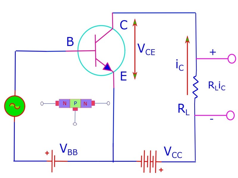
The common emitter circuit (of a npn transistor) has its input (Base-emitter) forward biased and its output (collector-emitter) reverse biased.
The common emitter circuit (output) has a supply voltage VCC, load resistance RL and a current iC. Lets apply Kirchhoff’s 2nd law to this circuit; vCE = VCC – RLiC or 
This represents a straight line when plotted between iC and vCE. If we work out a little bit we see the straight line is characterized by its famous parameters, the slope, x-intercept and y-intercept; slope: -1/RL, x-intercept: VCC and y-intercept: VCC/RL.
This we obtained as follows:
- (a) for iC = 0, vCE = VCC this gives x-intercept.
- (b) for vCE = 0, iC = VCC/RL this gives y-intercept.
- (c) slope of y = mx + c is m, so for
it is -1/RL.
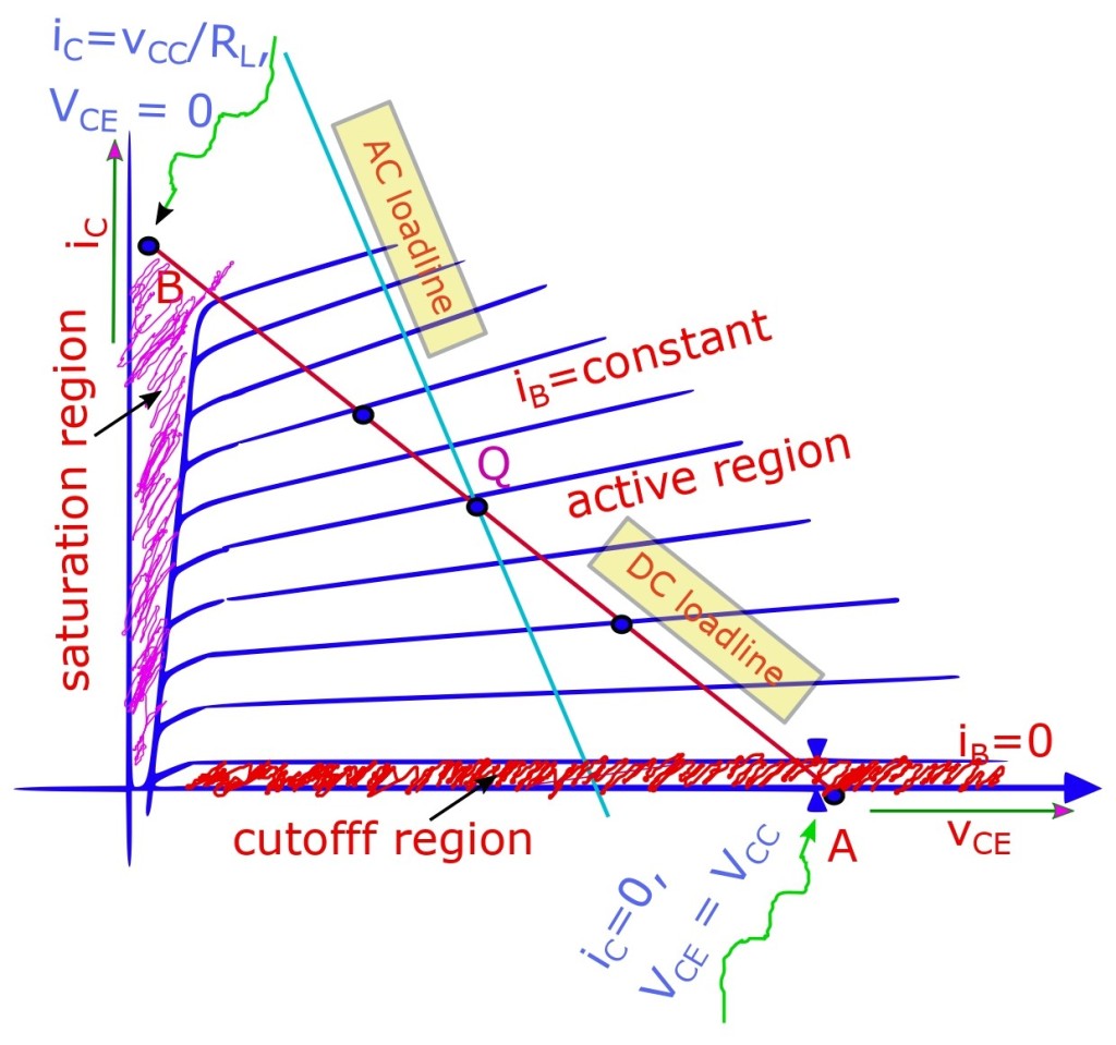
Lets now plot the npn output characteristics curves in this configuration and draw the straight line given by the Kirchhoff’s law. On it the x-intercept is marked as A and y-intercept is marked as B.
The DC load line against the output characteristics. Q-point, the saturation, active and the cutoff regions are determined from the output characteristics of the npn transistor in the common emitter configuration.

- The line joining the points A and B which represent the x and the y intercepts respectively [i.e. A: (x)y=0 = VCC and B: (y)x=0 = VCC/RL] is known as the static or DC load line. It is the locus of all possible pairs of values for iC and vCE, which can exist for specified given values of VCC and RL (which are fixed for a given circuit).
- The load line depends only upon VCC and RL values and is independent of the transistor output characteristics. The slope of the load line is -1/RL as we determined earlier.
- The load line intersects with the base current curve (characteristic curve) at the operating point: also known as the quiescent point, abbreviated as Q-point (shown as Q on diagram). This is because it is obtained when input ac signal is not applied. (zero that is). There is no amplification in this situation.
- Thus load line is a locus of all operating points with values of iB, iC and vCE that can exist for given values of VCC and RL.
Cutoff and Saturation.
cutoff
The point where DC load line intersects the iB = 0 curve is known as the cutoff point, at this point base-current is zero, collector current is negligible. Normal transistor action is lost, hence the name cutoff.
Active region is defined at one end by the cutoff which is obtained by reverse bias for both emitter and collector junctions. (i.e. input and output circuit) 
saturation
This is the point where load line intersects with iB = (iB)saturation curve. Here iC is the maximum. 
In the active region (DC load line directly gives this operational region) the amplifier is said to follow linear behavior. The faithful amplification is possible when the amplifier operates at its Q-point, i.e. at this point of operation complete portions of input signal (AC) is obtained by increasing signal strength.
Summary of constructing the DC load line.
- sum all the resistances in the emitter-collector circuit. Negative reciprocal of this sum gives slope of load line.
- sum of all voltage sources in emitter-collector circuit gives x intercept ( or point A: cutoff point)
- ratio of x-intercept to sum of resistances gives the y-intercept (or point B: saturation).

Leave a comment