
Analog systems and applications — lecture-XXI & XXII.
Analysis of a single stage common emitter (CE) amplifier and its hybrid equivalent circuit.
This article belongs to a series of lectures on analog electronics, the paper goes by the name “Analog Systems and Applications” for the physics honors degree class. All lectures of this series will be found here. This article comprises of the 21st and 22nd lectures of the series. The lectures were delivered on 28th March 2018.
In the discussions of the BJT so far we have discussed, their construction and working. It has been mentioned earlier that the BJT is capable of 2 functions, namely switching and amplification. It works under 3 regions of operations: active region which lies between the reverse-reverse biased cutoff region and forward-forward biased saturation region.
In addition we saw what happens when the BJT is biased, and discussed in detail two different ways that it can be biased in. Today we will see an application of all that we have learned so far. We will discuss today the single stage common emitter amplifier. We will also study the very interesting and useful idea of hybrid circuit analysis.
Lecture-21
Single stage amplifier
A single stage amplifier amplifies a weak signal but uses only a single transistor to achieve this. Lets discuss the case of a common emitter configuration circuit in detail.
This type of amplifier introduces a phase of 1800 between the input and the output signal. Lets draw a suitable diagram which utilizes a “voltage divider biasing” method which we discussed in out last lecture.
The common emitter circuit single stage amplifier. It consists of specially placed resistors for voltage divider type bias and capacitors for achieving desired actions.
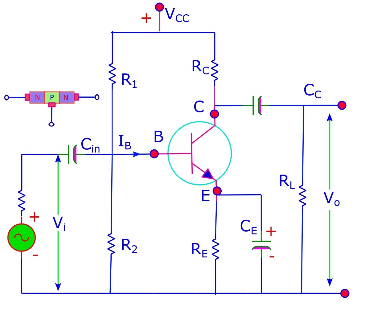
Single stage common emitter amplifier.
- Biasing circuit: The biasing circuit consists of action of 3 resistances, R1, R2 and RE. This circuit achieves stabilization for the amplifier by determining the operating point, in the active region, nearly at the middle of the AC load line — read more about operating point and load line, in this article.
- Input capacitor Cin: It couples the input signal Vi to the base of the transistor. It also allows the AC signal to flow, but blocks the DC component in Vi. DC biasing conditions are preserved by this capacitor, when AC signal is applied.
- Coupling capacitor CC: It is used to couple the output signal from the BJT to the load resistance RL. In multistage amplifiers, this capacitor couples one stage of amplification to the next stage. It isolates the DC component – in the AC, in one stage, from the next stage. It allows passage of AC signal from one stage to the next.
Cin and CC are called “blocking” or “coupling” capacitors, as they allow passage of AC signal but block the DC component in the signal.
- Emitter bypass capacitor CE: CE is connected parallel to the emitter resistance RE. Here reactance of the path via CE is low. Thus it acts like a bypass for the amplified AC signal. If CE is not utilized, AC signal through RE will suffer a drop in potential. This will feedback the AC input voltage. CE offers a reactance an order of magnitude smaller than RE, (XCE ≤ RE / 10) for lowest frequency in the input signal. Thus the output amplified signal chooses the low reactance path along CE. CE does not alter DC biasing condition.
- Load resistance RL: It is the total resistance of components connected to the output. Eg in case of multistage transistor based amplifiers input resistance of successive stage is the load resistance for the concurrent circuit.
Determination of currents.
- Base current: When Ac signal is not applied, the DC base current IB flows due to biasing. When AC signal Vi is applied, AC base current Ib flows through the base. Total base current is then given by:
. Here (IB) is DC and (Ib) is AC.
- Collector current: In absence of AC signal, DC collector current IC flows due to biasing. Upon application of AC signal, AC collector current Ic (AC with small letter subscript c) flows in addition to IC. Total collector current is then given by:
.
- Emitter current: Similar to the above occurrence the total emitter current is given by:
. Base current is usually very small; IE ≈ IC and Ie ≈ Ic (AC).
Mathematically it can be seen that: VCC = VCE + iCRC or VCE = VCC – ICRC – Ic(AC)RC or dVCE = – (dIc(AC))RC — as DC values are constant. So there is a phase lag of 1800 between input and output.
This also vindicates our earlier assertion.
- The DC load line can be determined as before. (See here) The AC load line can be determined by graphical method. Here Rac = RC || RL. Thus slope of AC load line is given by: -1/Rac = -(RC + RL)/ (RC*RL). The instantaneous operating points due to AC signal are no more constants. But AC load line goes through the DC Q point.
Lecture 22
Equivalent or Hybrid circuit method (h-parameter).
- Amplifiers can be analysed by segregating the total behavior into AC and DC equivalent circuits.
- For DC equivalent circuit, only DC conditions are considered. AC signal is replaced by internal impedance. Capacitors behave as open paths in circuits, and DC can’t pass through them.
- For AC equivalent circuit, only AC conditions are considered. DC sources are replaced by internal resistances.
- Capacitors are selected with large values. So for mid-frequencies, capacitors offer very low reactance (1/ωc).Then this corresponds to short circuits.
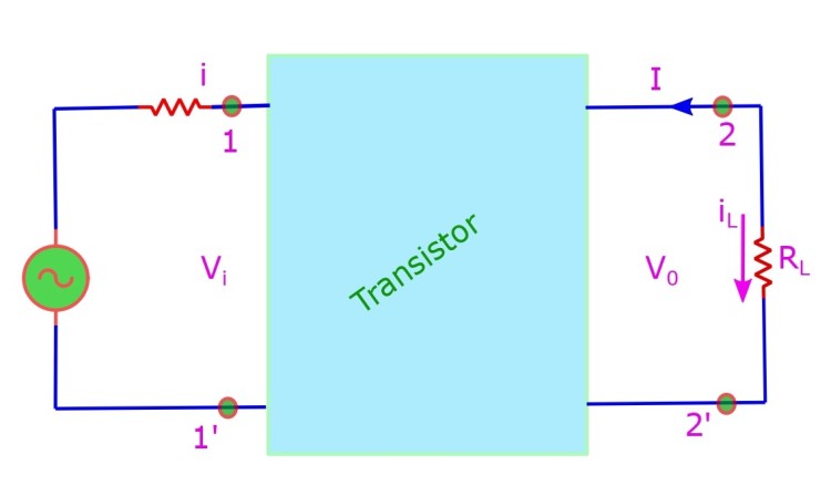
- For drawing and calculating AC behavior or AC equivalent circuit we use the 2-port network or hybrid-equivalent circuits. This uses definition of h-parameters as ensues in the following diagram and discussions.
The general amplifier circuit and the hybrid equivalent circuit. Various parameters by the name h-parameter are defined. More description of the method is given below.
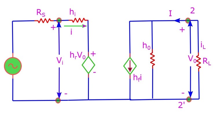
We see that there are various parameters now, hr, hf, hi and ho. These are known as h-parameters. Those of you who have a prescient nature might already have had a premonition; r stands for reverse (it appears with output voltage Vo and parameter hr in the input loop which are a feedback from the output loop) and f stands for forward (it appears with input current i and parameter hf in the output circuit, these are feedback from the input loop). Obviously in the subscripts: i stands for input and o stands for output.
Keep a mind which is defined where (in which loop) and supposed to act in which. An input defined h-parameter must act on an input variable and an output defined h-parameter must act on an output variable.
The h-parameters with r or f in their subscript must act on a variable that’s defined in the opposite loop. In other words one with r is actually defined in the forward loop — its a messenger from forward to reverse hence, r in the subscripT. similarly f in the subscript means its defined in the input loop but going to emigrate to output loop to show its action. hollaback.
Now we can write: Vi = (hi)i + (hr) Vo eqn 1 and I = (hf)i + hoVo eqn 2. Here i is the input current but I is the output current.
note that in eqn 1 hi is like a resistance variable whereas hr is a dimensionless feedback parameter.
similarly in eqn 2 hf is a dimensionless feedback parameter but ho is like a resistance variable.
For a common emitter (CE) configuration we will add an additional subscript e which will remind us we have a grounded emitter circuit. With the above discussions in mind our common emitter circuit drawn eg in our first diagram above, will look like the following in its hybrid avatar.
The common emitter single stage amplifier in its hybrid circuit form. Note the additional subscript e reminds us its a grounded emitter circuit.
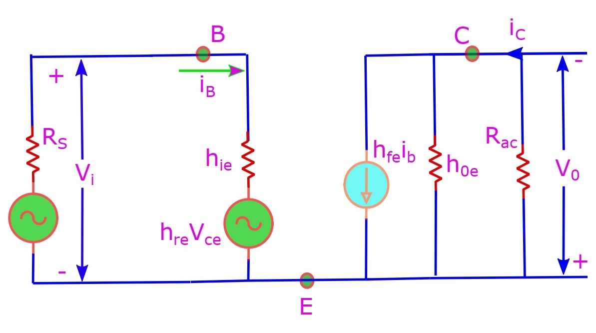
Input voltage source Vi is assumed to be ideal (this is known as first approximation i.e. zero internal resistance). ⇒ iB remains almost same, irrespective of resistances R1 and R2. Thus R1 and R2 are omitted in our circuit analysis. RL is parallel to RC thus the effective AC resistance is Rac = RC || RL = (RC*RL) / (RC + RL).
Lets use Kirchhoff’s law to the input loop in the above diagram. Basically we are adding subscript e to eqn 1. Vi = (hre) Vce + (hie)iB. Similarly when we do that to the output loop we obtain from eqn 2; iC = hoeVo + (hfe)iB.
Vo = – iC Rac (as iC flows upwards its negative).
Thus we have – Vo / Rac = hoeVo + (hfe)iB or Vo = -hfe iB Rac / (1+ hoeRac).
- Output Current:
.
- Current Gain:
.
We know that: Vce = Vo. (The bypass capacitor CE allows this.) Thus Vi = hieiB – hrehfe iB Rac / (1+ hoeRac).
This gives us the
- Voltage Gain:
. By using Rac = RC || RL = (RC*RL) / (RC + RL) we have another expression for voltage gain.
.
The negative sign indicates a phase reversal of 1800.
- Power Gain: power gain = current gain X voltage gain. So
.
- Input Impedance: Zie = input voltage Vi / input current iB.
. This depends on RL.
- Output Impedance: for this we recognize that RL is disconnected. ⇒ Rac = 0 so iC – hoeVo – hfeiB = 0. If RS is internal resistance of input source for input circuit: hreVce + iB ( hie + RS ) = 0. Vce = Vo. These two equations give:
. Thus output impedance is given by:
.
Source resistance (RS) decides output impedance. hre is small and hie is large for junction transistors. This leads to simplified expressions for voltage and power gain. so finally we have;
Current Gain:
Voltage Gain: 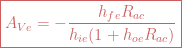
Power Gain: 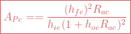

Leave a comment