
Transistor Biasing: Base resistor and Voltage divider bias.
Analog systems and applications — lecture-XIX & XX.
This article belongs to a series of lectures on analog electronics, the paper goes by the name “Analog Systems and Applications” for the physics honors degree class. All lectures of this series will be found here. This article consists of the 19th and the 20th lectures of the series. The lectures was delivered on 27th March 2018.
In the latest episodes of this series we discussed in fair detail and illustration the ideas of how two diodes can be combined to form bipolar junction transistors (BJT) that are capable of switching and amplification functions. We saw their characteristics in various configurations in our first two lectures (here). Then we discussed the 3 regions of operations in the BJT and discussed the special case of common base configuration in our 3rd lecture (here). In our last lecture (here) we discussed the load line analysis, Quiescent point and the 3 regions of operations, especially for the case of the common emitter configuration.
Now we would like to delve on the important basic concept of biasing a transistor. We have seen the details of biasing the diodes earlier (mainly here, and here, apart from in their applications in later lectures: such as various rectifiers, in LED and photodiodes and in Zener diode voltage regulator, you should assimilate exactly how the idea of biasing helps us achieve a wide variety of capabilities of the diodes).
Transistor Biasing.
Transistors operate as amplifiers when external DC supply voltages are used and a desired current IC is produced. The control voltage or current are known as “BIAS”.
Usually we need two biasing DC sources, one in the input circuit and one in the output circuit. But this is inconvenient and costly. We can instead use only one supply bias voltage: VCC.
There are various ways to achieve this type of biasing. Eg Biasing with (i) Base resistor (ii) Feedback resistor (iii) Emitter resistor (iv) Voltage divider
From among these four, we will discuss only (i) and (iv) ie. biasing with base resistor and voltage divider bias.
(i) Base resistor biasing.
This is also known as a “Base bias” or a “fixed bias” circuit.
- A single DC supply of voltage VCC is applied to both collector and base wrt emitter.
- Emitter is the reference level of voltage i.e its considered “grounded” or “earthed”.
- A high value of resistance RB (~ 100 kΩ or more) is connected between base and positive end of supply voltage VCC for n-p-n type transistors. For p-n-p type transistors RB is connected between base and negative end of supply voltage VCC.
The following diagrams show the circuits for both n-p-n and p-n-p type of transistors in the common emitter configuration.
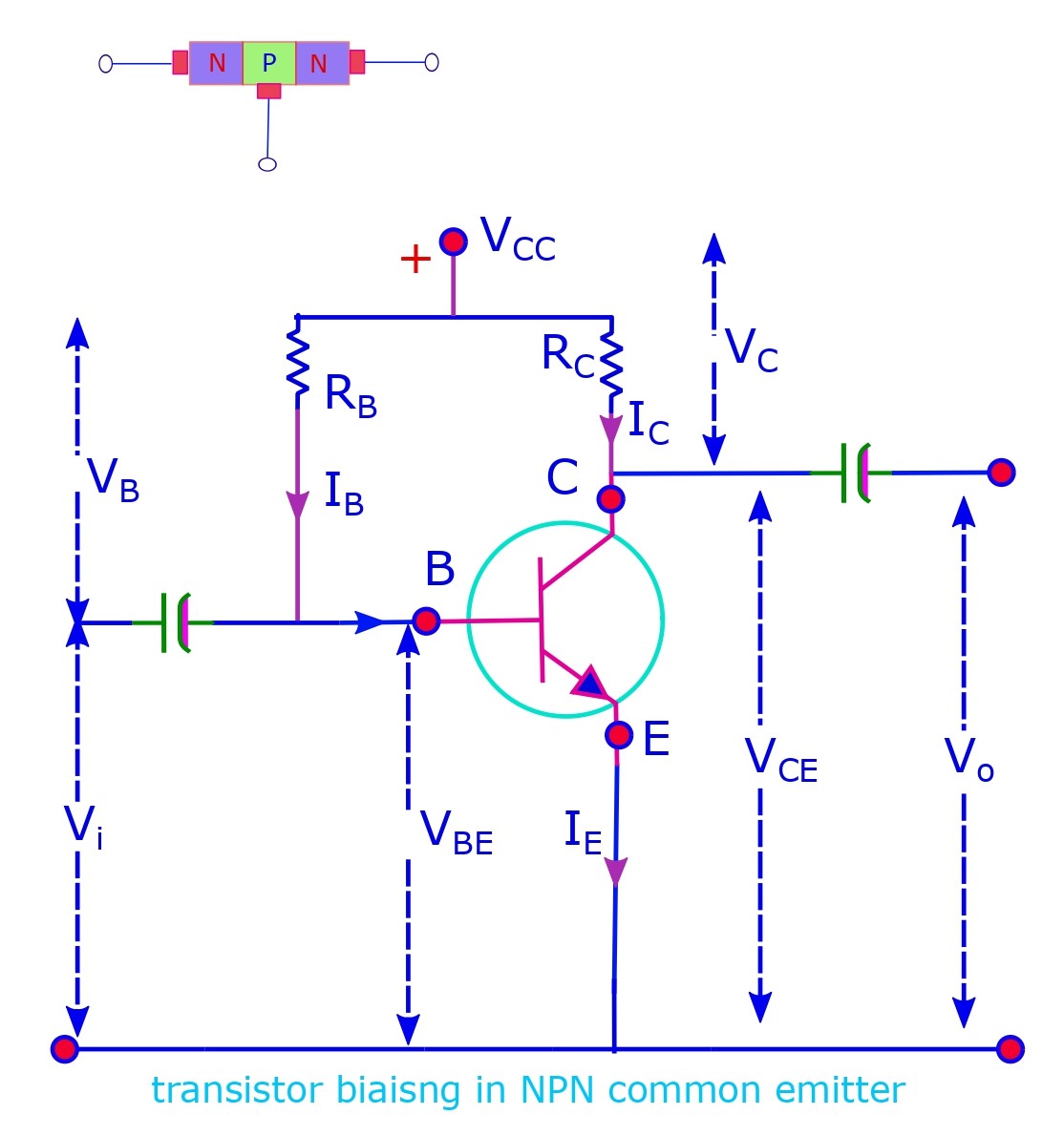

Note the sign of bias voltage is different wrt n-p-n and p-n-p type transistors in the same configuration this alters the direction of current flow as well.
- “Zero signal” base current IB can be achieved by selecting proper value of base resistor RB. If IC is “zero signal” collector current and β is the current gain, then; IC = βIB.
- Lets apply Kirchhoff’s law to the input loop, that is, base-emitter circuit. Then: VCC = IBRB + VBE ⇒ IB = (VCC – VBE)/RB. VBE is very small compared to VCC. eg VBE is 0.3 V for Ge and 0.7 V for Si. We can neglect VBE. Thus: IB = VCC / RB.
- Supply voltage VCC is fixed. Once RB is selected, base current IB is also fixed. This is the reason this mode of biasing is known as “fixed bias method”.
- Collector current in the output circuit is given as: IC = βIB + ICEO, where ICEO is the leakage current in the CE configuration. Although ICEO is not as small as ICBO, still a small error is entertained if ICEO is neglected. So, IC = βIB.
- Lets apply Kirchhoff’s law to the output circuit (i.e. collector-emitter loop). VCC = VC + VCE = ICRC + VCE. ⇒ ICRC ≤ VCC or IC ≤ VCC / RC. Thus (IC)max = VCC / RC, is known as saturation collector current: (IC)saturation. It is independent of the base current IB. In this situation: IC = βIB, is invalid.
How to determine operating point in fixed bias?
- Know VCC, select RB, IB calculated: IB = VCC / RB. If VBE is known more precise equation: IB = (VCC – VBE)/RB can be used.
- IC calculated from: IC = βIB (Using available transistor data for β). Its verified that IC ≤ (IC)saturation (from IC ≤ VCC / RC).
- VCE is calculated from VCC = ICRC + VCE.
Advantage
- Circuit is very small, only 2 resistances and 1 battery are required. Only one resistance (RB) fixes the operating point.
- No resistance is required across base-emitter junction.
- Biasing point and Q-point can be easily set by adjusting value of RB.
Disadvantage
This type of circuit is not used very often, for following reasons:
- Operating point depends on β. When β is large, transistor operates in saturation region and linear amplification is not produced.
- Poor stabilization: Q-point varies due to individual variation (e.g. replacement of transistor with a different one) or thermal runaway (i.e. variation of temperature)
- Stability factor is very high. It indicates likelihood of thermal runaway.
(ii) Voltage divider biasing
- It is the most extensively used biasing method. The reason is it has a very high degree of bias stability even when β and leakage current are high.
- Two resistances R1 and R2 are connected across supply bias voltage VCC as shown in the diagram below. R1 and R2 form a voltage-divider, the reason why this type of biasing is known as “voltage divider biasing”. Voltage drop across R2, forward biases emitter diode, hence the name “emitter bias” or “self bias” are also used for these type of circuits.
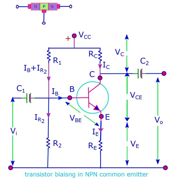
The voltage divider biasing shown for a n-p-n type transistor in its common emitter configuration.
- Lets apply voltage-divider rule in the input circuit to determine V2 across R2.
eqn 1.
- Kirchhoff’s voltage law, in the base circuit gives V2 = VE + VBE =IERE + VBE. eqn 2. Or, IE = (V2– VBE) / RE eqn 3.
- Kirchhoff’s (voltage) law applied to the output circuit : VCC = VC + VCE + VE = ICRC + VCE + IERE. eqn 4. IC and IE are approximately equal (since IB << IC). Thus; VCC = VCE + IC ( RC + RE ). This gives: VCE = VCC – IC ( RC + RE ) and IC = (VCC – VCE) / ( RC + RE ).
- Thus β does not appear in any of the above equations. Operating point is independent of β of transistor. Replacement of transistor does not affect operating point.
- Effect of temperature change: Increasing temperature will increase IC. This causes “voltage drop across emitter resistance RE” to increase. But voltage drop across R2 is independent of IC. Thus VBE must decrease. This increases IB which in turn decreases IC. This makes voltage divider bias circuit as a very suitable one for many applications.
- (IC)saturation = VCC / (RC + RE). (VCE)cutoff = VCC. DC load line has intercepts; vertical: VCC / (RC + RE) and horizontal: VCC.

Leave a comment