Analog systems and applications, lecture — V
“Energy levels in semiconductors.”
This article belongs to a series of lectures on analog electronics, the paper goes by the name “Analog Systems and Applications” for the physics honors degree class. All lectures of this series will be found here. This is the fifth lecture of this series. This particular lecture was delivered on 10th January 2018.
Today we will discuss about energy levels and energy bands in semiconductors as well as breakdown in reverse bias.
You might first wanna have a look into what we already discussed in this series of lecture. This will help you spruce up for the material to be discussed today.
- semiconductors and charge carriers lecture-I
- semiconductors and charge carriers lecture-II
- conductivity and mobility in semiconductors lecture-III
- PN junction diodes lecture-IV
Energy Level.
The energy of an electron is proportional to the size of the orbit it is found in. Thus specifying the radius of an orbit, of the electron, is equivalent to specifying its energy level. So electrons in the smallest or innermost orbit are in the first energy level. Electrons in the next higher orbit. i.e. second orbit belong to the second energy level, which is higher. Thee next orbit corresponds to the next energy level which is still higher, and so on for higher orbits and energy level.
This is because there is an attractive interaction between the nucleus and the electrons. Electrons must gain energy to go into higher energy levels. This is achieved by sources of heat, light or applied potentials. When the electrons fall from the higher energy levels they release their extra energy again in the form of heat, light or other radiation.
This is the working principle behind semiconductor based LED. The applied potential raises the electrons to their higher energy levels. These electrons then emit light of red, green, orange or infrared wavelength etc when de-excited.
Energy Bands.
An isolated atom has electrons whose energy level depends upon the interaction between the electrons and the nucleus to which these electrons are attached. These energy levels look like lines drawn on an energy axis, corresponding to the different orbits we just discussed. 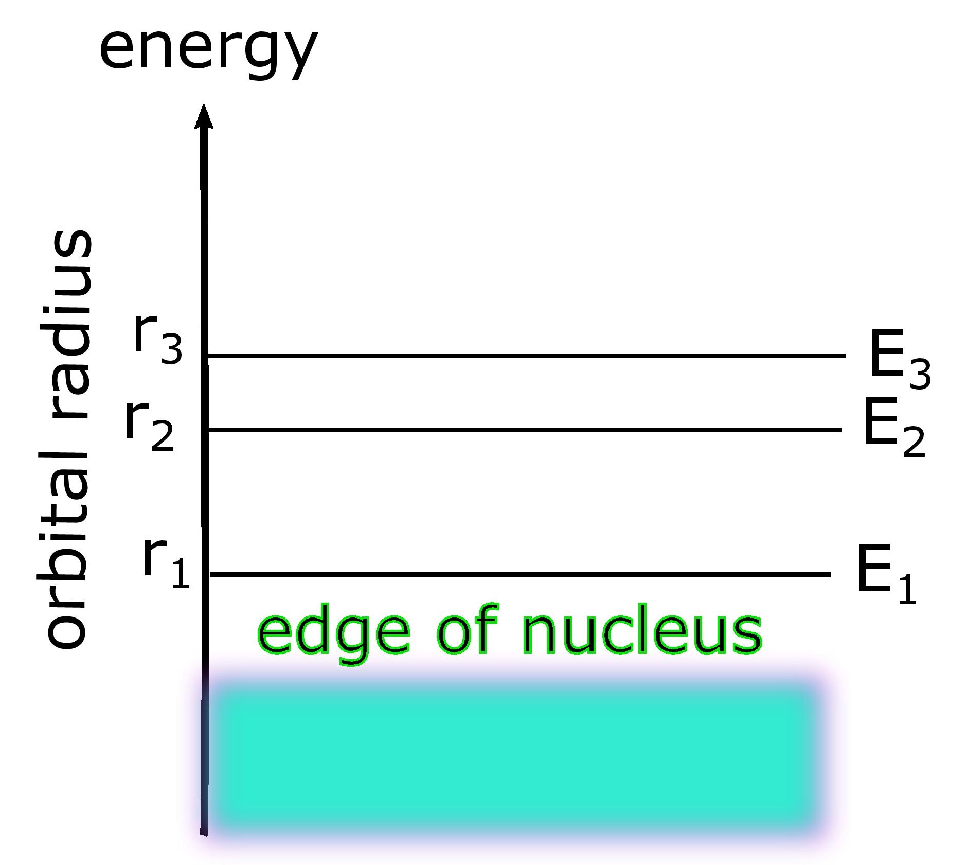
What happens when there are a large number of atoms, instead of just a single atom, as in a crystal?
Now the electrons in a particular atom are influenced by a multitude of other atoms in the neighborhood of the original atom. Thus each electron is governed by a different value of energy as their charge environments are different from each other.
In other words instead of a single line on the energy axis in an energy level diagram, there are a large number of different lines, quite close to each other.
Thus the energy level of a single atom keeps on splitting to multiple values with successive addition of atoms. Eventually for a very large number of atoms, as found in a semiconductor crystal, for example, bands of energy levels appear instead of single lines of energy levels. These are therefore known as “Energy bands“.
It is obvious that electrons in the first energy level of their respective atoms give rise to an energy band appropriate for the first energy level of each electron, which corresponds to the smallest orbit. The next band forms at a higher energy level corresponding to the next higher orbit and so on.
A similar logic is sufficient to see that energy bands are stipulated for electrons found in valence energy levels and also for conduction energy level, in a semiconductor.
The holes created in a semiconductor crystal thus remain in the valence band and free electrons can jump to the conduction band, due to higher available energy to them. 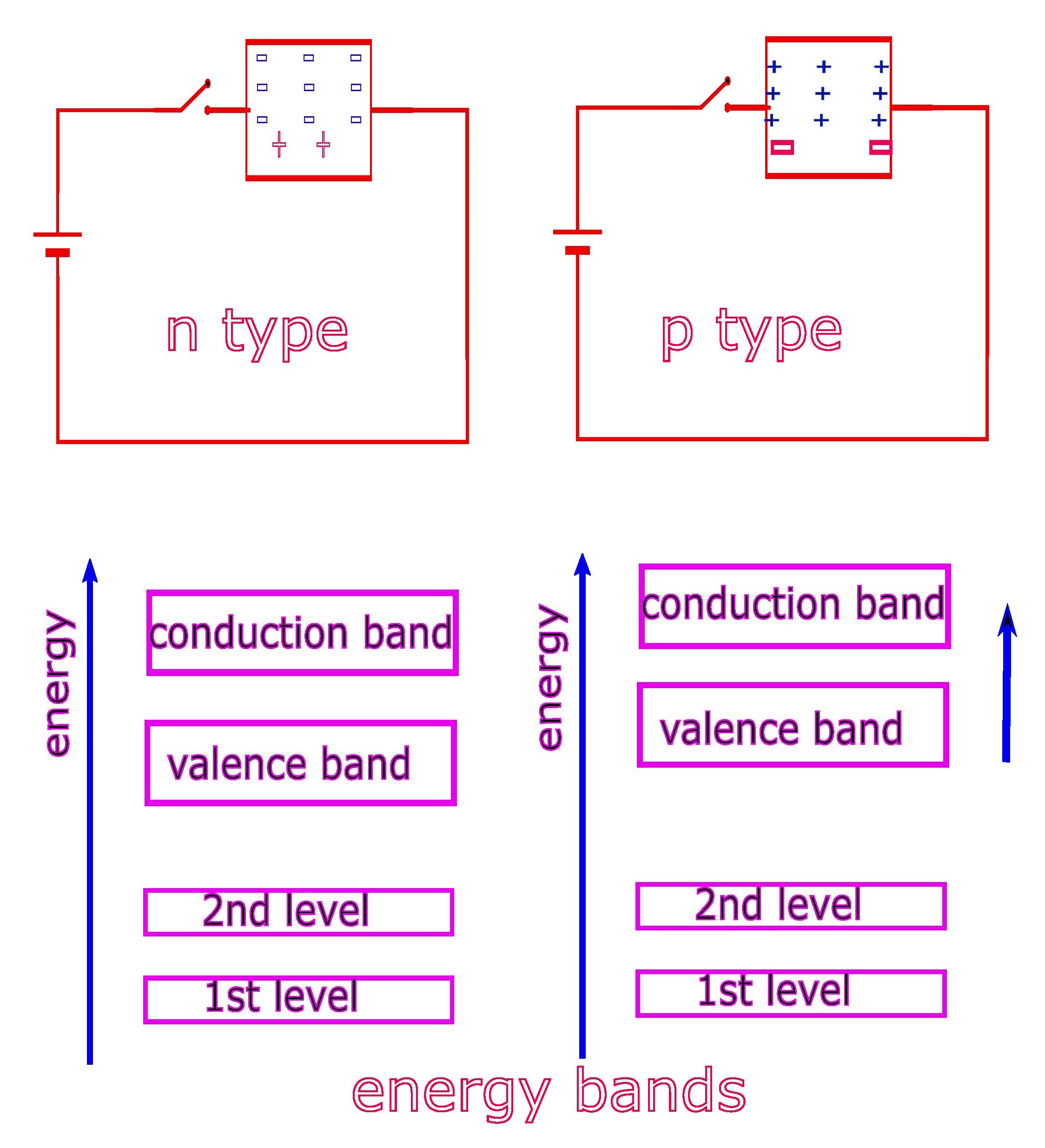
Energy Hill.
The properties of pn junction devices are greatly determined by the energy levels of its constituent carriers under different conditions.
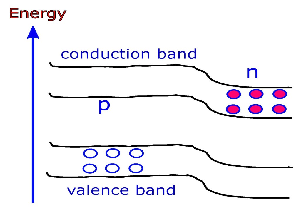
Before diffusion of electron takes place in a pn device, the p-bands (bands on p-side) are slightly higher than the n-bands. This is because p-side has trivalent atoms (lets say with a core charge of +3). Similarly n-side has pentavalent atoms (lets say with a core charge of +5). Consequently the conduction and valence orbits are smaller for n-type configuration than for p-type.
When a depletion layer develops this further adds the energy difference between p-side and n-side: for both conduction and valence bands. This is because recombination of electrons and holes forces conduction band to be higher than valence band. 

That means due to depletion it becomes more difficult for electrons in n-side to cross over to the p-side and recombine. This is equivalent to saying an energy hill develops due to depletion at the junction. We need to supply energy to the free electrons to overcome this hill.
Thus during forward bias the electrons gain extra energy and the hill is reduced in height. But reverse bias increases the hill further and it becomes more difficult to climb the hill than it is due to depletion.
Break down in reverse bias.
When reverse bias voltage is increased beyond certain value, the electrons which were pushed away from depletion layer, so that depletion layer widened, gain a lot of energy. These minority carriers knockoff an extra electron from the valence bands which were previously not free. This increases the number of free carrier electrons.
The process continues in geometric fashion and is known as avalanche effect. One free electron produces two, two free electrons produce four and so on. Reverse current thus increases by large amount and diode may undergo breakdown. Usually this does not happen below 50 V.

Leave a comment