
Analog systems and applications, lecture — VI.
“Barrier potential and width in a pn step junction, L-VI.”
This article belongs to a series of lectures on analog electronics, the paper goes by the name “Analog Systems and Applications” for the physics honors degree class. All lectures of this series will be found here. This is the sixth lecture of this series. This particular lecture was delivered on 25th January 2018.
Today we will discuss about the depletion region in greater detail than before. We will derive a quantitative relation among barrier potential and its width which are created in the depletion region, as discussed before. We will also derive an expression for the electric field that is established due to this potential.
So far we have the following 5 lectures in this series. You might wanna have a look through them, before or after reading this, for greater connectivity and assimilation of ideas.
- Semiconductors and charge carriers lecture-I
- Semiconductors and charge carriers lecture-II
- Conductivity and mobility in semiconductors lecture-III
- PN junction diodes lecture-IV
- Energy levels in semiconductors lecture-V
Lets first recall how electric field and electric potential are related to each other. Electric field is the negative potential gradient. Mathematically, in 1 dimension this is expressed by the following formula.

In 3 dimensions it can be written as 
We also know the Gauss law in electrostatics which has an integral form: 


Lets us now use the definition of the electric field (

In 3 dimensions this equation would look like: 
In a medium we have to replace ε0 by ε, the permittivity of the medium, the Poisson’s equation becomes: 
Let us now assume ND to be the constant density of ionized ‘donor’ atoms, which extends to distance x1, into n-region and NA to be the constant density of ionized ‘acceptor’ atoms, which extends to distance -x2 into p-region. 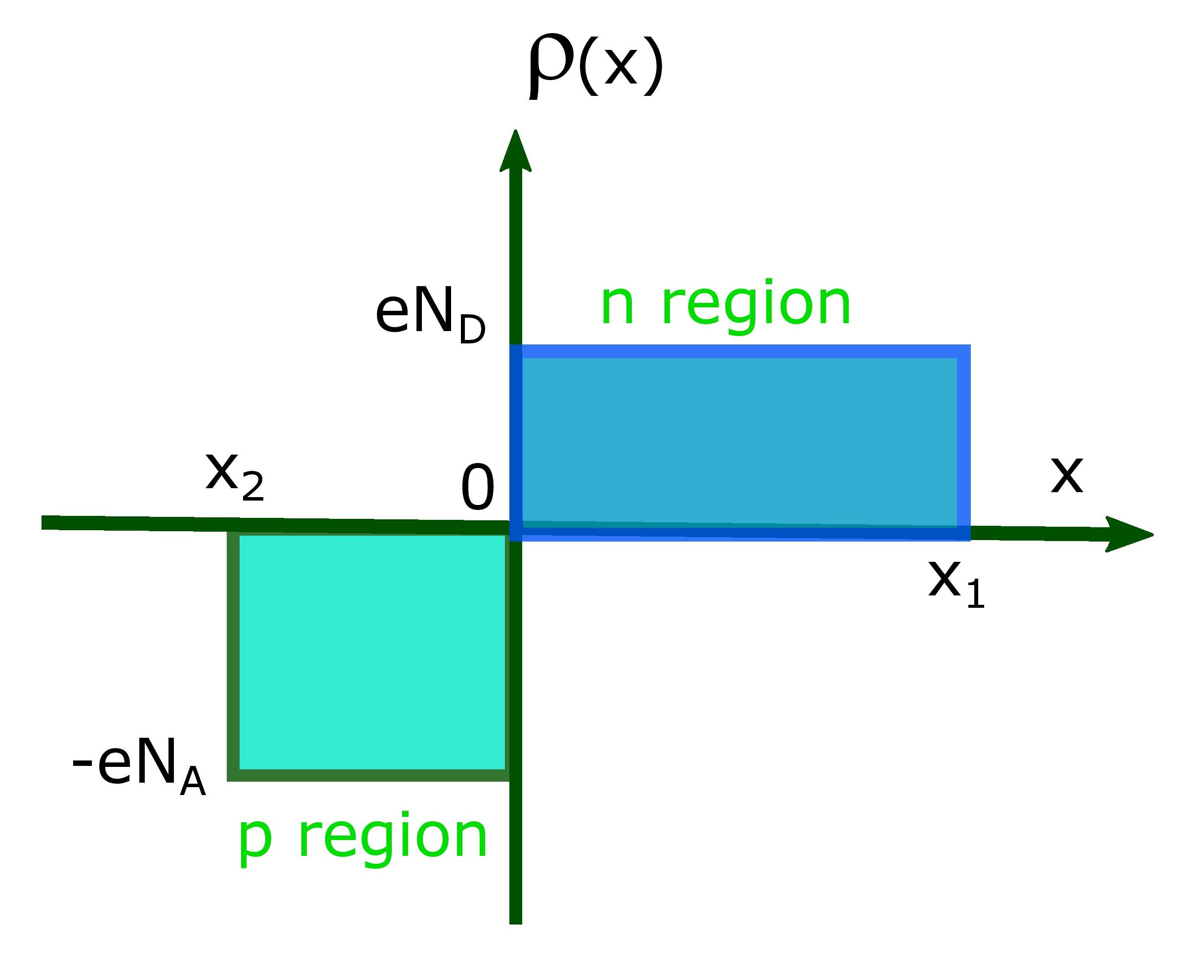
Let us also assume that the concentrations of electrons (n) and holes (p) are negligible in the “depletion region“. So, we have two equations for each region of the pn junction. One for the n-region and one for the p-region.


Electric field variation.
Let us now integrate ( eqn 2 ) & ( eqn 3 ). This gives us ( eqn 4 ) in n-region and ( eqn 5 ) in p-region.


Potential is constant at the boundaries ( x = x1 and x = x2 ) as shown in the figure. i.e. 

Since “electric field is negative potential gradient” from ( — eqn 4 ) we have: 

The field in each region increases as x approaches “zero” i.e. the junction. Electric field at the junction then is given by: 
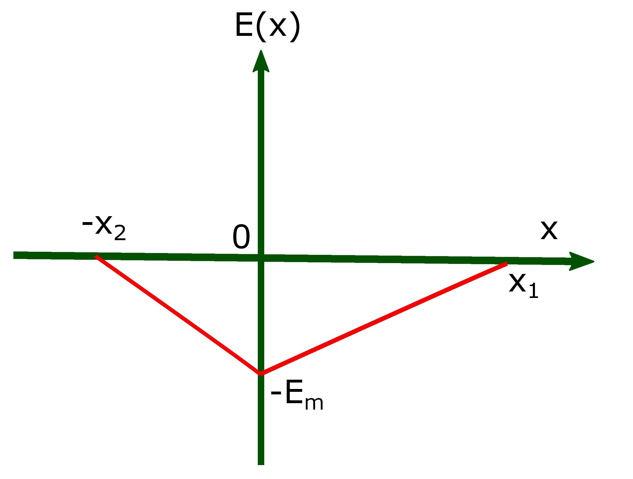
From “charge conservation” we have; 
Thus at the junction (x=0) 
‘0’ stands for equilibrium and x0 ( = x1 + x2 ) is known as “width of the depletion region”.
Potential variation.
Let us integrate ( — eqn 4 ) & ( — eqn 5 ); and use the defining relation 


Now let is use the boundary conditions. The potential is zero where the depletion layer begins at the p-side (x=-x2) and it is same as the builtin potential where depletion region ends on n-side (x=x1). Mathematically: 

Then from the 2nd boundary condition above: 

This gives us the expression for the potential in the entire n-region. ![\boxed{V_n(x) = -\frac{eN_D}{\epsilon}[\frac{x^2}{2}+\frac{{x_1}^2}{2}-xx_1]+V_B}](https://s0.wp.com/latex.php?latex=%5Cboxed%7BV_n%28x%29+%3D+-%5Cfrac%7BeN_D%7D%7B%5Cepsilon%7D%5B%5Cfrac%7Bx%5E2%7D%7B2%7D%2B%5Cfrac%7B%7Bx_1%7D%5E2%7D%7B2%7D-xx_1%5D%2BV_B%7D&bg=ffffff&fg=cd5c5c&s=1&c=20201002)
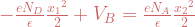
From the 1st boundary condition above: 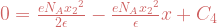

This gives us the expression for the potential in the entire p-region. ![\boxed{V_p(x) = \frac{eN_A}{\epsilon}[\frac{x^2}{2}+\frac{{x_2}^2}{2}+xx_2]}](https://s0.wp.com/latex.php?latex=%5Cboxed%7BV_p%28x%29+%3D+%5Cfrac%7BeN_A%7D%7B%5Cepsilon%7D%5B%5Cfrac%7Bx%5E2%7D%7B2%7D%2B%5Cfrac%7B%7Bx_2%7D%5E2%7D%7B2%7D%2Bxx_2%5D%7D&bg=ffffff&fg=cd5c5c&s=1&c=20201002)
Junction potential and width of depletion layer.
The potential V must be continuous at the junction (x=0). This implies 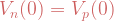

![V_B = \frac{e}{2\epsilon}[1+ \frac{N_A}{N_D}]N_A {x_2}^2=\frac{e}{2\epsilon}[1+ \frac{N_D}{N_A}]N_D {x_1}^2](https://s0.wp.com/latex.php?latex=V_B+%3D+%5Cfrac%7Be%7D%7B2%5Cepsilon%7D%5B1%2B+%5Cfrac%7BN_A%7D%7BN_D%7D%5DN_A+%7Bx_2%7D%5E2%3D%5Cfrac%7Be%7D%7B2%5Cepsilon%7D%5B1%2B+%5Cfrac%7BN_D%7D%7BN_A%7D%5DN_D+%7Bx_1%7D%5E2&bg=ffffff&fg=cd5c5c&s=1&c=20201002)
Let us now solve for x1 and x2.
![x_1 = [\frac{2\epsilon N_A V_B}{e (N_A+N_D)N_D}]^{\frac{1}{2}}](https://s0.wp.com/latex.php?latex=x_1+%3D+%5B%5Cfrac%7B2%5Cepsilon+N_A+V_B%7D%7Be+%28N_A%2BN_D%29N_D%7D%5D%5E%7B%5Cfrac%7B1%7D%7B2%7D%7D&bg=ffffff&fg=cd5c5c&s=1&c=20201002)
![x_2 = [\frac{2\epsilon N_D V_B}{e (N_A+N_D)N_A}]^{\frac{1}{2}}](https://s0.wp.com/latex.php?latex=x_2+%3D+%5B%5Cfrac%7B2%5Cepsilon+N_D+V_B%7D%7Be+%28N_A%2BN_D%29N_A%7D%5D%5E%7B%5Cfrac%7B1%7D%7B2%7D%7D&bg=ffffff&fg=cd5c5c&s=1&c=20201002)
This gives us the total depletion width or the asymmetric step junction width: 
For symmetric step junction: x1 = x2 = x0/2 and NA = ND = N. Then: 
For one sided step-junction, one side of pn junction is heavily doped, eg, if p-region is heavily doped then x2 << x1 as NA >> ND. Then; 
If donors on n-side are all ionized, electron conductivity σn in terms of its mobility is given by: 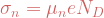
This implies: 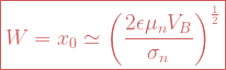
Peak electric field can be obtained from the plot of electric field shown earlier (triangles). Area of triangle (VB) is half the base (x0) times height (Em) So, 

Leave a comment