Analog systems and applications — lectures – XXVI, XXVII.
This article belongs to a series of lectures on analog electronics, the paper goes by the name “Analog Systems and Applications” for the physics honors degree class, — click on link to left to access all lectures of this series. This article comprises of the 26th and 27th lecture of the series. The lectures were delivered on 3rd April 2018.
This is our 12th lecture in this series where we are dealing with the witty transistors. They must be something in the electronics industry. In our last 5 lectures (lectures 21, 22, 23, 24 and 25) we discussed in good detail the frequency response of the single stage RC coupled common emitter amplifiers apart from their circuit details, operations and analysis like Miller’s theorem and hybrid circuit method, and voltage and power gain etc.
Before that in 6 lectures we had dwelled on their basic nature and conditions under which they perform in desirable ways (such as biasing). Now the time has arrived when we can look into how transistors are classified into various types, of which there are a great many. In doing so we will attain a greater level of understanding of these tiny marvels. Remember how they had outwitted the hulk mighty vacuum tubes in some sort of electronics war.
Classification of power amplifiers into class A, B, C amplifiers, lectures 26 & 27.
Electronic systems need voltage amplification followed by power amplification. It is the voltage of output after signal is amplified to higher voltage level which drives the power amplifier.
Transistor of high β (corresponds to thin base) is used for voltage amplifiers. But small β (which corresponds to thick base) are used in power amplifiers.
According to conservation of energy power amplifiers can’t increase the power of the transistor. They take the DC power and convert it into AC power.
This is the reason they are known as power converter or frequency converter.
Good voltage amplifiers are not good power amplifiers. Power transistors must be built with good heat dissipation capabilities. Therefore the size of the collector region of power transistors must be large.
There are 3 types power amplifiers based on the manner in which a transistor is operated: class A, class B and class C — we won’t discuss whats called the class AB, we will just mention in passing what they are. Now we will discuss the first 3 types of amplifiers in detail.
Classification of class A, B, C amplifiers.
The amplifiers can be classified into various classes, according to the point of operation i.e. biasing. We will see how the manner of operation is different for different classes. There are 4 classes that are defined; A, B, AB and C, (and there are many more types). Of these we will study only class, A, Class B and class C in detail.
- Class A amplifier: In this class of amplifiers, the transistor conducts over the entire cycle. Thus the output replicates the input signal waveform.
- Class B amplifier: In such a class of amplifiers, the transistor conducts only over one-half cycle. For the rest of the cycle the transistor is switched off or cutoff.
- Class AB amplifier: This is a class of amplifier, where the transistor operates intermediate of class A and class B amplifiers. The transistor conducts for more than half (more than B) but less than 1 (less than A i.e.).
- Class C amplifier: This is another basic class of amplifier like class A and class B. Here transistor conducts for less than half cycle (less than B i.e.).
Lets now study in detail the class A, B, and C type of power amplifiers.
Class A amplifier
We will study their circuit diagram, characteristics, power efficiency, advantages and disadvantages. The following diagram shows a “single ended transformer coupled, class-A, power amplifier” circuit.
In this circuit, as in many electronic circuits, a loud speaker serves as the load in the power amplifiers. The load has a low impedance. The collector circuit has a high impedance on the other hand. A voltage step-down or current step-up transformer serves two purposes.
- (i) to transfer power to the loudspeaker.
- (ii) to provide impedance matching.
To understand point (ii), remember the transformer mechanism: RL‘ = (N1/N2)2 RL.
(N1 > N2) (step down) ⇒ RL‘ > RL. A transformer with proper turns ratio, therefore, matches low impedance RL with high output impedance RL‘. [or ro]
Power transformers are large signal amplifier. In such conditions they are no more linear devices. Transistor parameters are no more constant. Therefore AC equivalent circuit can’t be used for circuit analysis.
We resort to graphical method instead.
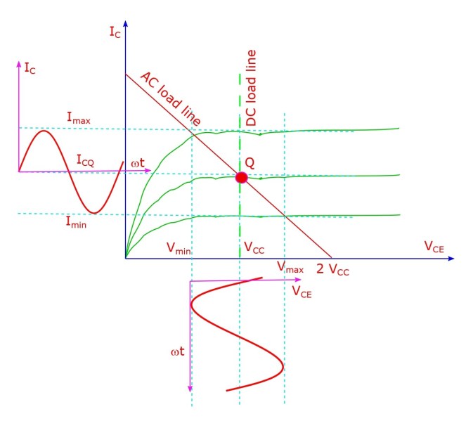
Under zero signal conditions, DC resistance of primary of the transformer is assumed to be zero. Also RE is small. DC load-line is almost a vertical line, passing through the operating point Q, where VCE = VCC, iC = ICQ. AC load line also goes through Q, and has a slope of: tan-1 (-1/RL‘).
Positive and negative peaks may not be equal (i.e. peaks can be asymmetric). i.e. Imax – ICQ ≠ ICQ – Imin and Vmax – VCC ≠ VCC – Vmin.
DC input power, Pi = AC output power Po + Power loss PD.
Pi = Pdc = VCC × IC(av).
Lets assume symmetric peaks (below and above ICQ). Since, IC(av) = ICQ, so Pi = VCC × ICQ.
There is no loss of power, in transformer: Po = secondary power = Primary power.
AC output power Po = Vrms × Irms = Irms2RL‘.
Average peak value of current, Io = 1/2 [(Imax – ICQ) + (ICQ – Imin)] = 1/2 [Imax – Imin]
⇒ Irms = (Imax – Imin) / 2√2.
Similarly Vrms = (Vmax – Vmin) / 2√2. Thus Po = 1/8 (Vmax – Vmin) (Imax – Imin).
VCC = (Vmax + Vmin) / 2 and ICQ = (Imax + Imin) / 2.
⇒ Pi = VCC × ICQ = 1/2 (Vmax + Vmin) × 1/2 (Imax + Imin) = 1/4 (Vmax + Vmin) (Imax + Imin).
Thus efficiency of class A power amplifier: 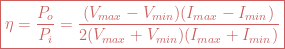
η is always less than 50 % for class A type amplifiers. The maximum occurs when operating point of signal goes from 2 ICQ to 0 and collector voltage goes from 0 to 2 VCC.
So, 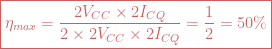
Po (max) = maximum output power = 1/8 (2VCC . 2ICQ) = 1/2VCC . ICQ = 1/2 ICQ2RL‘ as VCC = ICQ RL‘.
Practically power efficiency of class A amplifiers is ≤ 35 %.
Disadvantages
- Power efficiency is too low.
- Batteries are used, this is not cost-effective.
- Harmonic distortion is too high, mostly second harmonic.
- Amplifier minimizes distortion, at the cost of output.
- Saturation problem in output power transformer, due to DC current in primary.
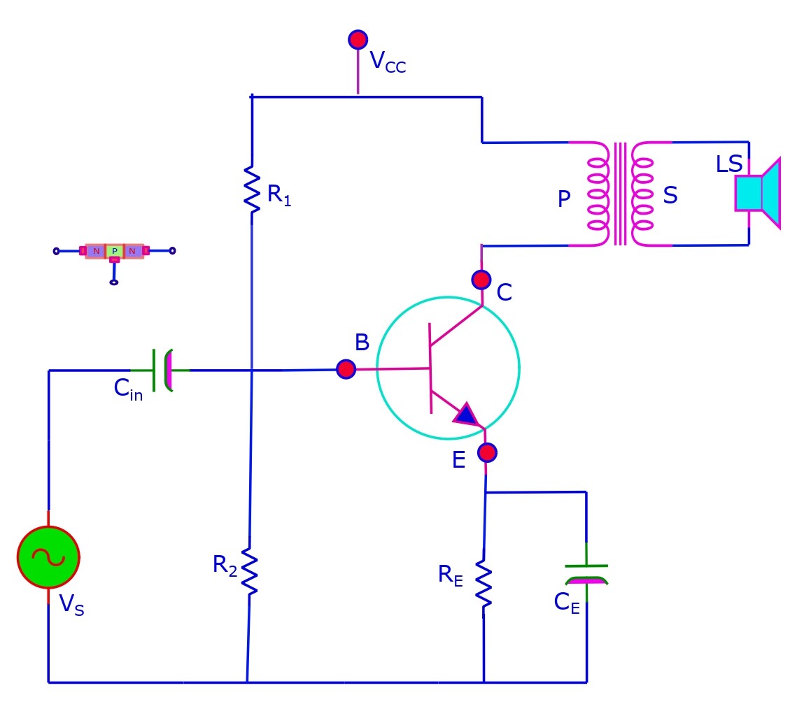
Push-Pull class B amplifier
It uses two identical amplifier transformers. The input signal to them is 1800 out of phase by a center-tapped input transformer. Also the output transformer is center-tapped. The disadvantage of class A amplifier are removed. The circuit can work as a class A, AB or B amplifier, as suits the purpose. Two n-p-n transistors are used in parallel or back-to-back.
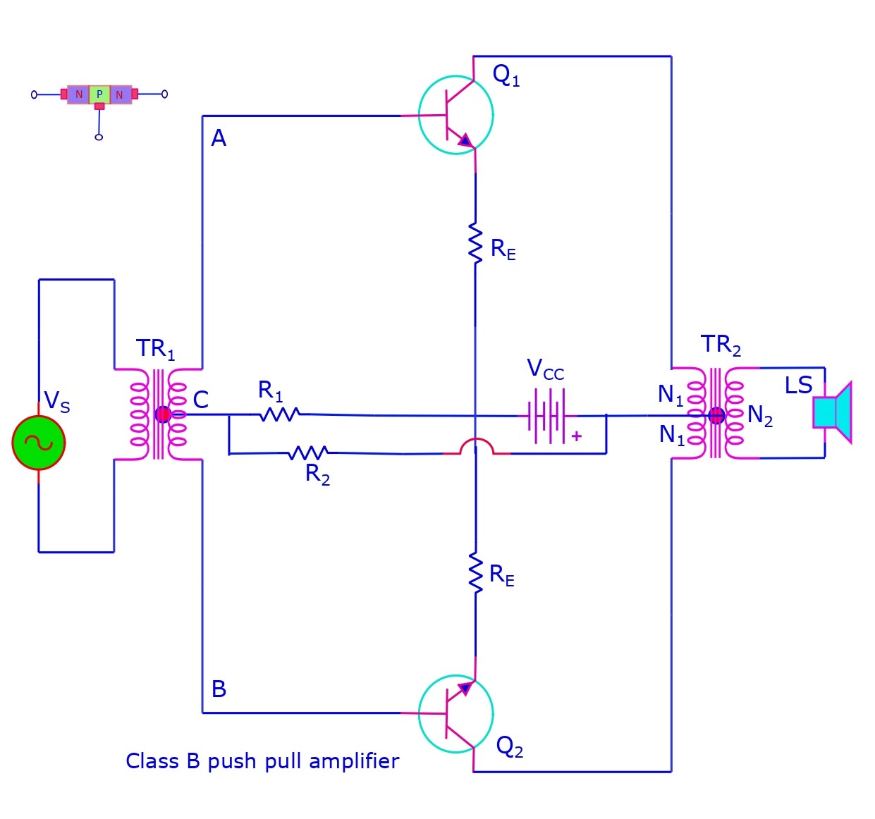
Input signal drives the two transistors Q1 and Q2 on alternate half-cycles (transformer TR1 provides opposite polarity to them). DC supply VCC is applied to the center tap of the output transformers primary. Turn ratio 2 N1/N2 is chosen to match RL with RL‘. R1 and R2 control the operational point’s proximity to cutoff. RE (actually two of them) are temperature compensating resistors.
During first half-cycle (lets say A is +ve and B is -ve) Q1 will conduct (as its forward biased). The converse occurs during second half cycle, and Q2 conducts (which was earlier reverse biased but now forward biased).
Since during one-half cycle only one part of the amplifier has a current which replicates the input signal , its “pushed up“, the other part is “pulled down“. This reverses in the successive half cycle. This is why these are known as push-pull amplifiers.
Lets show the input voltage signal and the output current behavior of the signal in the amplifier by the following diagram.
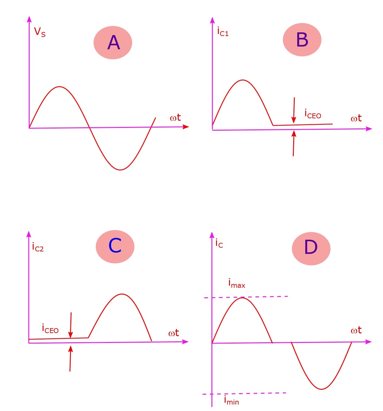
Diagram D shows the cross-over distortion at cutoff bias. This occurs because β is low at low collector current, i.e. near cutoff, compared to the rest of the cycle. Both transistors (Q1 and Q2) can be slightly forward biased, by default, to overcome cross-over distortion. This is achieved by choices of R1 and R2. This takes us slightly off from class B towards class A. Thus its designated as class AB.
Power conversion efficiency: it can be shown with some basic equations that (refer eg to electronics book by Tayal and Tayal from Himalayan publication) 
For ideal cases: Vmax – Vmin = 2VCC and Imax – Imin = 2Imax = 2VCC / RL‘.
Thus, 
Po (max) = maximum output power = 1/2 (VCC . Imax) = VCC2 / 2RL‘.
Po (diss) = power dissipated = Pi – Po = 2 (VCC . Imax)/π – (Vmax – Vmin)(Imax – Imin)/8.
For ideal case: Po (diss) = (2/π) VCC . Imax – 1/2 RL‘ Imax2.
So maximum power dissipated is obtained by differentiating the above: Po (diss, max) = (2/π2) VCC / RL‘.
Transistor utilization factor (figure of merit) 
(For now you can check for advantages/disadvantages from the same book referred above, I might also make an attempt to update this if its possible soon).
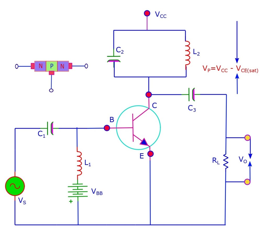
Class C amplifier
It is used only for a single frequency input or a narrow band of input frequency. Tuning is done by means of a parallel LC circuit. Resonance frequency is given by: 
Collector current flows for less than 1800 of input cycle. There is heavy distortion. Single pulse outputs die out after some time, so a narrow current pulse is used, with each pulse bringing the transistor to switch on state. Following is the circuit diagram for a class C amplifier.
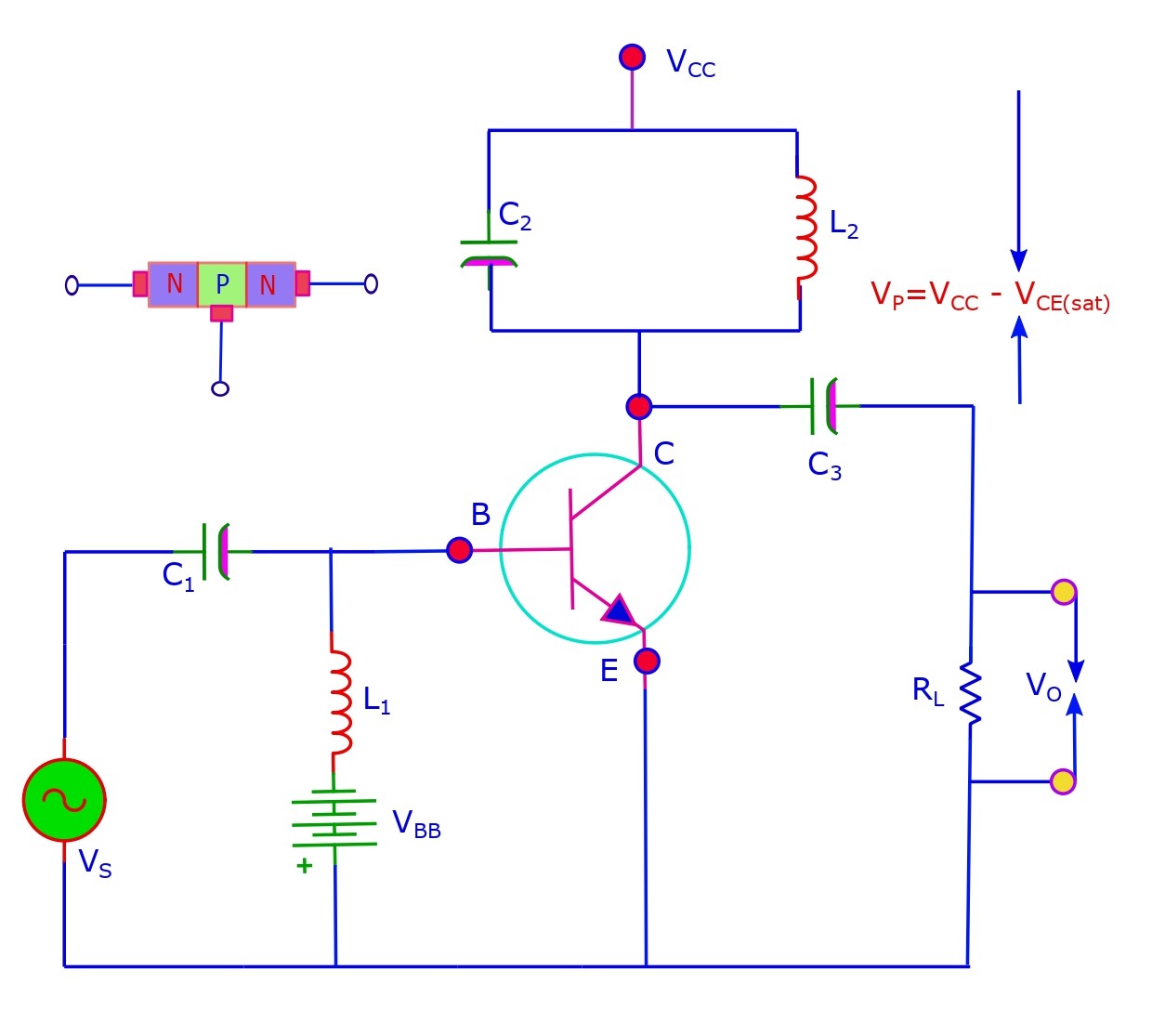
Base is reverse biased (-ve VBB) through L1, this keeps device in normally off state. VS > VBB will make it conduct. Thus IB, IC flow only when AC input signal peak is slightly greater than |VBB|+VBE.
Po= VP2 / 2RL, VP ~ VCC.

Practically its 85 %.

Leave a comment