
Analog systems and applications — lectures – XXIV, XXV.
Single stage common emitter RC coupled amplifier at high frequency, Lecture 24 and 25.
This article belongs to a series of lectures on analog electronics, the paper goes by the name “Analog Systems and Applications” for the physics honors degree class, — click on link to left to access all lectures of this series. This article comprises of the 24th and 25th lecture of the series. The lectures were delivered on 2nd April 2018.
RC coupled amplifier in high frequency range.
In our last lecture we discussed the case of a single stage RC coupled amplifier, a common emitter transistor circuit, for its response at low frequencies, i.e. frequencies that are less than 50 Hz. Today we will discuss what changes are going to be effected in the same circuit when we pass signal at high frequency. We defined high frequency in our last lecture to be one which is higher than 20 kHz.
- In the depletion layers at the junctions of the CE transistor that we have been discussing, capacitance are developed due to depletion. (Read more about depletion layer here.) These capacitance are denoted by Cbe, Cbc and Cce according to the terminals they appear across. They can’t be neglected in general when the frequency of signal is high.
- Cbe: its the internal capacitance of the forward biased emitter-base junction. It offers a low impedance in the input side, at high frequency application of signal.
- Cbc: its the internal capacitance of the reverse biased collector-base junction. It connects output with input and provides negative feed-back.
- Cce: its the internal capacitance between the collector and the emitter, it produces a shunting effect in the output side, at high frequency.
- Cw1 and Cw2: these are the wiring capacitance, as shown in the following diagram. These are small valued capacitance but their reactance are significant at high frequencies.
- CE and CC: and CE is the bypass capacitor and it is considered sufficiently large so that its reactance at high frequency is negligible. Reactance of CC is also negligible.

Miller theorem and Miller effect
When an impedance Z is connected from output to the input of an inverting amplifier with voltage gain A, Z may be replaced by an input Miller impedance: Z/A+1 and an output Miller impedance: (ZA)/A+1.
A schematic that depicts the Miller’s theorem stated above is shown in the following diagram.

Miller’s theorem: An impedance shared between input and output can be replaced by an equivalent circuit where the impedance is replaced by an input effective impedance and an output effective impedance.
When Z is replaced by a capacitance C, Miller’s theorem dictates C(1+A) as the input capacitance and C(1+A)/A as the output capacitance.
Thus total input capacitance of our transistor circuit is: Cin = Cbe + (1 + Av) Cbc. This input impedance, at high frequency, for a single stage amplifier is small and can be neglected.
But in the output of the first stage, it increases due to presence of strong wiring capacitance Cw2 and input capacitance of second stage Cin. Thus: Cs = Cce + Cw2 + Cin.
Hybrid equivalent circuit for high frequency response is shown below.

Now we can find the voltage gain etc as before in the case of medium and small frequency — see linked articles.
Applying Kirchhoff’ (voltage) law to the input loop: Vi – hreVce = hieib.
Applying Kirchhoff’s current law at node C, in the output circuit: hfeiB + hoeVo + Vo/RC + Vo/RL jωCSVo = 0.
Lets use the fact: Vce = Vo and solve for Vo. As before we obtain: 
Now we can divide this (AV,h) by the voltage gain at mid-frequency, AV,m that we derived earlier, as we did before for low frequency voltage gain.
![\boxed{\frac{A_{V,h}}{A_{V,m}}=\Bigg[1+j\frac{2\pi f C_S h_{ie}}{h_{ie}(h_{oe} +\frac{1}{R_C}+ \frac{1}{R_L})-h_{re}h_{fe}}\Bigg]^{-1}}](https://s0.wp.com/latex.php?latex=%5Cboxed%7B%5Cfrac%7BA_%7BV%2Ch%7D%7D%7BA_%7BV%2Cm%7D%7D%3D%5CBigg%5B1%2Bj%5Cfrac%7B2%5Cpi+f+C_S+h_%7Bie%7D%7D%7Bh_%7Bie%7D%28h_%7Boe%7D+%2B%5Cfrac%7B1%7D%7BR_C%7D%2B+%5Cfrac%7B1%7D%7BR_L%7D%29-h_%7Bre%7Dh_%7Bfe%7D%7D%5CBigg%5D%5E%7B-1%7D%7D&bg=ffffff&fg=cd5c5c&s=0&c=20201002)
Thus
- (i) gain at high frequency is less than gain at med-frequency,
- (ii) gain decreases with increase in frequency due to shunt capacitance CS,
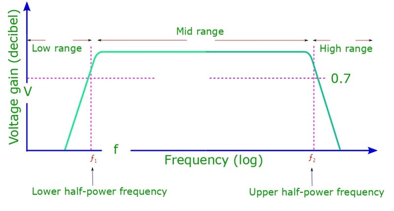
- (iii) as before we can define an upper cutoff frequency fh = f2.
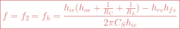


Thus at f = f2, |AV,h / AV,m| = 1/√2 = 0.707 ≡ 70.7 % as in the case of low-frequency cutoff, the gain drops to a level of this percentage of maximum gain, as given by this factor, at this upper cutoff frequency. Total phase shift of voltage gain in high frequency range is given by: φh = 1800 – θl = 1800 – tan-1 (f/fh). At f = f2, φh = 1800 – 450 = 1350.
Now the circuit behaves like a low pass RC circuit. Effective resistance is given by: Then 
For small value of hoe, hre 
Thus this is a parallel combination of the shunt resistances in the collector circuit.
The voltage gain in decibel vs frequency in a log scale is known as the Bode plot.
Here is the definition of a decibel: Decibel power gain = 10 log10 (PoPi) = 10 log10 AP.

Leave a comment